
Chopped wave band-gap reference device with switched-capacitor filter

A technology of switched capacitors and reference equipment, which is applied to instruments, regulating electrical variables, and control/regulating systems, etc., can solve problems such as reducing the noise performance of reference circuits, limiting low-noise applications of circuits, and difficult to obtain reference voltages, and improving stability. stability and precision, the effect of reducing the impact

Inactive Publication Date: 2015-02-25
芯动科技(珠海)有限公司
View PDF10 Cites 4 Cited by
  • Summary
  • Abstract
  • Description
  • Claims
  • Application Information

AI Technical Summary

Problems solved by technology

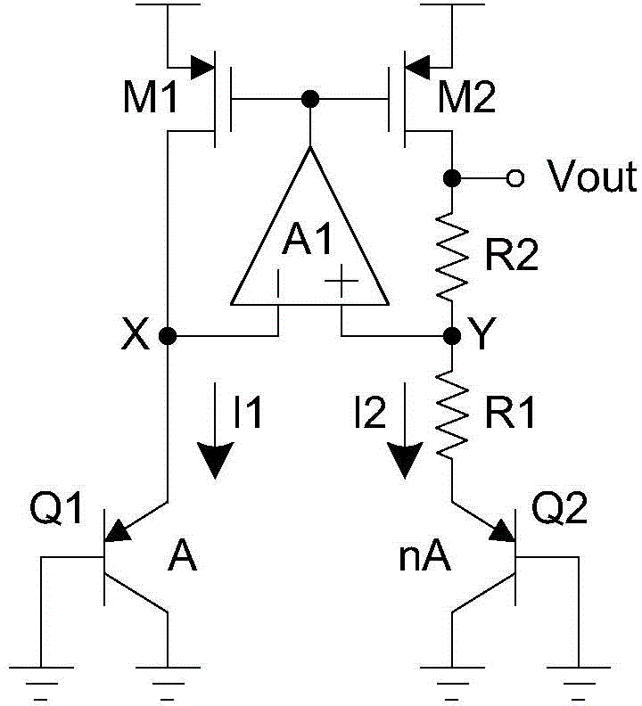
Through the above analysis, it can be seen that the noise of the op amp appears directly at the output terminal. At the same time, since the reference circuit works at the DC level, and the low frequency 1 / f noise is particularly large compared with the high frequency thermal noise, the 1 / f noise of the op amp Noise can significantly degrade the noise performance of the reference circuit, limiting the circuit's low-noise applications
Moreover, there are large differences in the size and parameters of devices under different process environments, so it is actually difficult to obtain a reference voltage with zero temperature coefficient at room temperature, and the zero temperature coefficient point may even be far away from room temperature. Due to asymmetry, the operation The amplifier will be affected by the input offset voltage, which means that the input of the op amp is zero but its output voltage is not zero, thus affecting the stability and accuracy of the reference voltage

Method used


Image

  • Chopped wave band-gap reference device with switched-capacitor filter
  • Chopped wave band-gap reference device with switched-capacitor filter
  • Chopped wave band-gap reference device with switched-capacitor filter

Examples


Embodiment Construction

[0022] The following description and drawings illustrate specific embodiments of the invention sufficiently to enable those skilled in the art to practice them. Other embodiments may incorporate structural, logical, electrical, process, and other changes. The examples merely represent possible variations. Individual components and functions are optional unless explicitly required, and the order of operations may vary. Portions and features of some embodiments may be included in or substituted for those of other embodiments. The scope of embodiments of the present invention includes the full scope of the claims, and all available equivalents of the claims. These embodiments of the present invention may be referred to herein, individually or collectively, by the term "invention", which is for convenience only and is not intended to automatically limit the application if in fact more than one invention is disclosed The scope is any individual invention or inventive concept.

...


PUM


Abstract

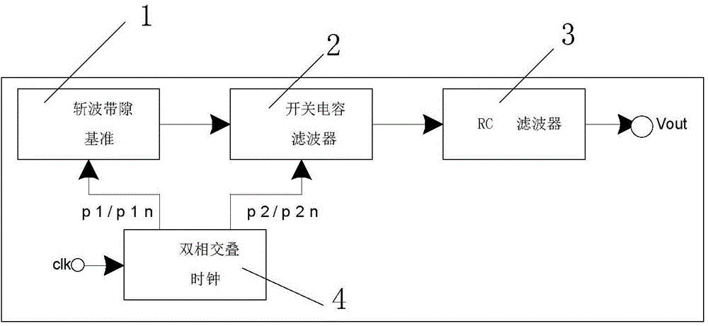
The invention discloses a chopped wave band-gap reference device with a switched-capacitor filter. The chopped wave band-gap reference device with the switched-capacitor filter comprises a chopped wave band-gap reference device body, wherein the output end of the chopped wave band-gap reference device body is connected with the input end of the switched-capacitor filter, the output end of the switched-capacitor filter is connected with the input end of an RC filter, and a reference voltage output port is formed in the output end of the RC filter. An output voltage regulating component formed by connecting at least three resistors in series is arranged in the chopped wave band-gap reference device. The chopped wave band-gap reference device is further provided with a biphase overlapping clock device, wherein the input end of the biphase overlapping clock device is provided with an external clock input port, and the biphase overlapping clock device is provided with at least two clock signal output ends. The voltage regulating component is formed by connecting multiple resistors in series instead of one resistor, and thus final output voltage which is originally fixed is made adjustable; the influence of offset voltage on reference voltage is eliminated through filtering, noise at the low frequency 1 / f of a chopped wave operational amplifier is converted to noise at the clock frequency, the influence of the noise at the low frequency 1 / f is greatly reduced after filtering, and both the stability and the accuracy of the reference voltage are improved.

Description

technical field [0001] The invention belongs to the field of bandgap reference circuits, in particular to a chopping bandgap reference device with a switched capacitor filter. Background technique [0002] A typical bandgap reference circuit in the prior art such as figure 1 As shown, the principle is: it is composed of resistors, transistors, MOS tubes and operational amplifiers, where R1 and R2 represent resistors; M1 and M2 are generally two PMOS transistors of the same size; A1 represents operational amplifiers; Q1 and Q2 represent pnp Transistors, wherein Q2 is generally composed of n parallel transistor units, and Q1 is generally one transistor unit. When the bandgap reference circuit works normally, the amplifier A1 makes its two input terminals: X and Y nodes, stabilized at approximately equal voltages. Among them, Vout represents the final output reference voltage. Since the MOS transistors M1 and M2 have the same size, the currents I1 and I2 are equal in magnitu...

Claims


Application Information

Patent Timeline
IPC IPC(8): G05F1/56
Inventor 黄实敖海敖钢
Owner 芯动科技(珠海)有限公司
Learn More