A kind of anti-potential induced decay solar cell and preparation method thereof

A technology of potential-induced attenuation and solar cells, which is applied in the field of solar cells, can solve problems such as unsatisfactory anti-PID performance, unsatisfactory sodium ion blocking effect, and reduced photoelectric conversion efficiency of solar cells, so as to improve the anti-PID effect and improve Effect of photoelectric conversion efficiency and improvement of anti-PID performance

Active Publication Date: 2018-02-06
GUANGDONG AIKO SOLAR ENERGY TECH CO LTD +1
View PDF6 Cites 0 Cited by
  • Summary
  • Abstract
  • Description
  • Claims
  • Application Information

AI Technical Summary

Problems solved by technology

Photons propagate from low refractive index media to high refractive index media to avoid total reflection of light and reduce light reflection; however, since the refractive index of silicon dioxide is about 1.5 and that of silicon is about 3.42, silicon nitride’s The refractive index is generally not greater than 2.0. Therefore, when photons propagate in air / silicon nitride / silicon dioxide / silicon, due to the low refractive index of silicon dioxide, light is prone to total reflection at the interface of silicon dioxide. The optical mismatch phenomenon will reduce the photoelectric conversion efficiency of solar cells; in addition, the anti-PID performance of single-layer silicon dioxide is not ideal, which does not meet the market's demand for anti-PID battery performance
[0004] In the prior art, there is also a silicon dioxide film with a refractive index higher than 2.0, but the refractive index of the silicon dioxide film can only be set to be no greater than 2.5, and the refractive index of the silicon oxide layer and the silicon nitride layer are still relatively low. The effect of sodium ions is not ideal, and the resistance to potential induced decay of the battery is not very ideal

Method used


Image

  • A kind of anti-potential induced decay solar cell and preparation method thereof
  • A kind of anti-potential induced decay solar cell and preparation method thereof

Examples


preparation example Construction

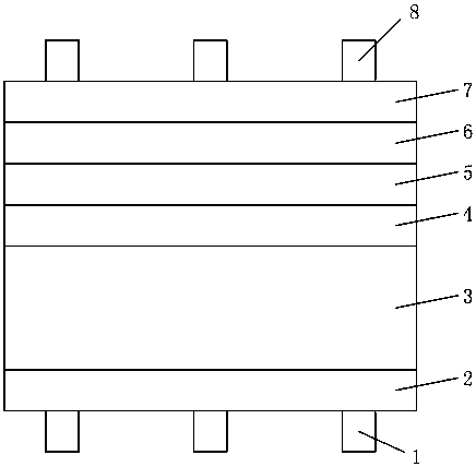
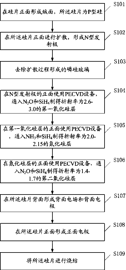
[0045] see figure 2 , the invention provides a method for preparing a solar cell resistant to potential-induced decay, comprising:

[0046] S101, forming a textured surface on the front surface of the silicon wafer, where the silicon wafer is P-type silicon.

[0047] The textured surface of the silicon chip adopts HF and / or HNO 3 solution to form an ideal suede structure and reduce reflectivity.

[0048] S102, performing diffusion on the front surface of the silicon wafer to form an N-type emitter.

[0049] The N-type emitter can be formed by methods such as thermal diffusion or ion implantation, wherein the diffusion of the silicon wafer is preferably made of phosphorus oxychloride.

[0050] S103, removing the phosphosilicate glass formed in the diffusion process.

[0051] Removing the phosphosilicate glass is beneficial to ensure the photoelectric conversion efficiency of the battery.

[0052] S104, use PECVD equipment on the front of the N-type emitter, and pass throu...

Embodiment 1

[0067] Forming a suede surface on the front side of the silicon wafer, the silicon wafer is P-type silicon;

[0068] Diffusion is performed on the front side of the silicon wafer to form an N-type emitter;

[0069] Removal of phosphosilicate glass formed by the diffusion process;

[0070] Use PECVD equipment on the front of the N-type emitter, pass N 2 O and SiH 4 A first silicon oxide layer with a refractive index of 2.6 and a thickness of 1nm was prepared, wherein the reaction temperature was 350°C, the deposition time was 10s, and the N 2 O and SiH 4 The flow ratio is 0.1:3;

[0071] Use PECVD equipment on the front side of the first silicon oxide layer, pass NH 3 and SiH 4 A silicon nitride layer with a refractive index of 2.10 and a thickness of 50nm was prepared, wherein the reaction temperature was 380°C, the deposition time was 500s, and SiH 4 and NH 3 The flow ratio is 0.1:1;

[0072] Use PECVD equipment on the front side of the silicon nitride layer, pass N ...

Embodiment 2

[0077]Forming a suede surface on the front side of the silicon wafer, the silicon wafer is P-type silicon;

[0078] Diffusion is performed on the front side of the silicon wafer to form an N-type emitter;

[0079] Removal of phosphosilicate glass formed by the diffusion process;

[0080] Use PECVD equipment on the front of the N-type emitter, pass N 2 O and SiH 4 A first silicon oxide layer with a refractive index of 2.65 and a thickness of 3nm was prepared, wherein the reaction temperature was 380°C, the deposition time was 50s, and N 2 O and SiH 4 The flow ratio is 0.5:5;

[0081] Use PECVD equipment on the front side of the first silicon oxide layer, pass NH 3 and SiH 4 A silicon nitride layer with a refractive index of 2.11 and a thickness of 52nm was prepared, wherein the reaction temperature was 400°C, the deposition time was 600s, and SiH 4 and NH 3 The flow ratio is 0.2:1;

[0082] Use PECVD equipment on the front side of the silicon nitride layer, pass N 2 O...


PUM


Abstract

The invention discloses a solar cell with potential induction decay resistance. The solar cell comprises back-surface electrodes, a back-surface electric field, P (positive)-type silicon, an N (negative)-type emitting electrode, a first silicon oxide layer, a silicon nitride layer, a second silicon oxide layer and front-surface electrodes. The first silicon oxide layer, the silicon nitride layer and the second silicon oxide layer are sequentially arranged on the N-type emitting electrode; a refractive index of the first silicon oxide layer ranges from 2.6 to 3.0; a refractive index of the silicon nitride layer ranges from 2.0 to 2.15, and a refractive index of the second silicon oxide layer ranges from 1.4 to 1.7. The invention further correspondingly provides a method for manufacturing the solar cell with the potential induction decay resistance. The solar cell and the method have the advantages that the front surface of the solar cell is of an overlaying structure with three layers of thin films, and accordingly the cell is excellent in potential induction resistance; refractive indexes of the overlaid layers are increased, accordingly, the solar cell is good in optical matching property and favorable for light absorption, excellent passivation effects can be realized, and the photoelectric conversion efficiency of the cell can be greatly improved.

Description

technical field [0001] The invention relates to the technical field of solar cells, in particular to a solar cell capable of resisting potential-induced attenuation and a preparation method thereof. Background technique [0002] Potential-induced degradation (PID) refers to the phenomenon that the power of solar cell modules decreases under the action of high temperature, high humidity and high voltage. Solar cell modules will experience different degrees of potential-induced attenuation phenomenon in about five years under the power generation state, which has become a major problem in the field of photovoltaic power generation. [0003] The cause of potential-induced attenuation is mainly due to the encapsulation material of the solar cell module - glass: the sodium ions inside the glass move to the solar cell, destroying the p-n junction of the cell, resulting in power attenuation. The hot spot of anti-potential-induced decay technology is silicon dioxide / silicon nitride...

Claims


Application Information

Patent Timeline
Patent Type & Authority Patents(China)
IPC IPC(8): H01L31/0216H01L31/04H01L31/18
CPCH01L31/02167H01L31/042H01L31/18Y02E10/50Y02P70/50
Inventor 石强秦崇德方结彬黄玉平何达能
Owner GUANGDONG AIKO SOLAR ENERGY TECH CO LTD
Why Eureka
Try Eureka