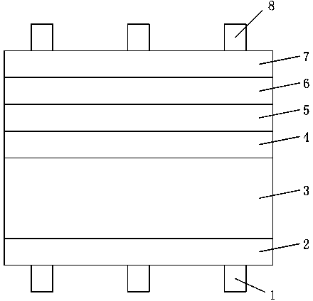
Solar cell with potential induction decay resistance and method for manufacturing solar cell
A potential-induced attenuation and solar cell technology, applied in the field of solar cells, can solve the problems of unsatisfactory sodium ion blocking effect, unsatisfactory anti-PID performance, and reduced photoelectric conversion efficiency of solar cells, so as to improve photoelectric conversion efficiency and improve Anti-PID effect, effect of improving anti-PID performance
- Summary
- Abstract
- Description
- Claims
- Application Information
AI Technical Summary
Problems solved by technology
Method used
Image
Examples
preparation example Construction
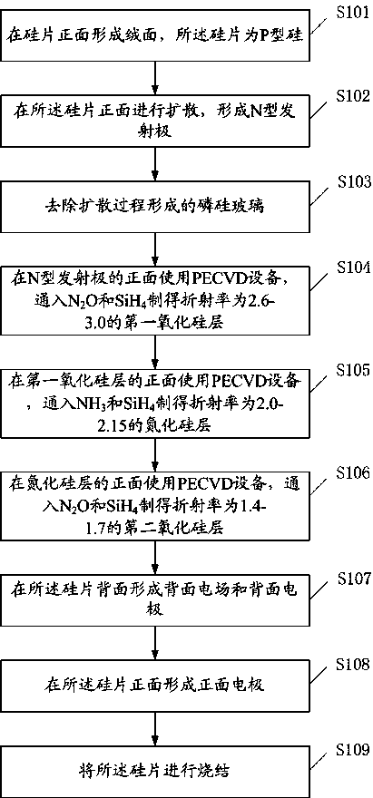
[0045] see figure 2 , the invention provides a method for preparing a solar cell resistant to potential-induced decay, comprising:
[0046] S101, forming a textured surface on the front surface of the silicon wafer, where the silicon wafer is P-type silicon.
[0047] The textured surface of the silicon chip adopts HF and / or HNO 3 solution to form an ideal suede structure and reduce reflectivity.
[0048] S102, performing diffusion on the front surface of the silicon wafer to form an N-type emitter.
[0049] The N-type emitter can be formed by methods such as thermal diffusion or ion implantation, wherein the diffusion of the silicon wafer is preferably made of phosphorus oxychloride.
[0050] S103, removing the phosphosilicate glass formed in the diffusion process.
[0051] Removing the phosphosilicate glass is beneficial to ensure the photoelectric conversion efficiency of the battery.
[0052] S104, use PECVD equipment on the front of the N-type emitter, and pass throu...
Embodiment 1
[0067] Forming a suede surface on the front side of the silicon wafer, the silicon wafer is P-type silicon;
[0068] Diffusion is performed on the front side of the silicon wafer to form an N-type emitter;
[0069] Removal of phosphosilicate glass formed by the diffusion process;
[0070] Use PECVD equipment on the front of the N-type emitter, pass N 2 O and SiH 4 A first silicon oxide layer with a refractive index of 2.6 and a thickness of 1nm was prepared, wherein the reaction temperature was 350°C, the deposition time was 10s, and the N 2 O and SiH 4 The flow ratio is 0.1:3;
[0071] Use PECVD equipment on the front side of the first silicon oxide layer, pass NH 3 and SiH 4 A silicon nitride layer with a refractive index of 2.10 and a thickness of 50nm was prepared, wherein the reaction temperature was 380°C, the deposition time was 500s, and SiH 4 and NH 3 The flow ratio is 0.1:1;
[0072] Use PECVD equipment on the front side of the silicon nitride layer, pass N ...
Embodiment 2
[0077]Forming a suede surface on the front side of the silicon wafer, the silicon wafer is P-type silicon;
[0078] Diffusion is performed on the front side of the silicon wafer to form an N-type emitter;
[0079] Removal of phosphosilicate glass formed by the diffusion process;
[0080] Use PECVD equipment on the front of the N-type emitter, pass N 2 O and SiH 4 A first silicon oxide layer with a refractive index of 2.65 and a thickness of 3nm was prepared, wherein the reaction temperature was 380°C, the deposition time was 50s, and N 2 O and SiH 4 The flow ratio is 0.5:5;
[0081] Use PECVD equipment on the front side of the first silicon oxide layer, pass NH 3 and SiH 4 A silicon nitride layer with a refractive index of 2.11 and a thickness of 52nm was prepared, wherein the reaction temperature was 400°C, the deposition time was 600s, and SiH 4 and NH 3 The flow ratio is 0.2:1;
[0082] Use PECVD equipment on the front side of the silicon nitride layer, pass N 2 O...
PUM
 Abstract
Description
Claims
Application Information
 - R&D Engineer
- R&D Manager
- IP Professional
- Industry Leading Data Capabilities
- Powerful AI technology
- Patent DNA Extraction
Browse by: Latest US Patents, China's latest patents, Technical Efficacy Thesaurus, Application Domain, Technology Topic, Popular Technical Reports.
© 2024 PatSnap. All rights reserved.Legal|Privacy policy|Modern Slavery Act Transparency Statement|Sitemap|About US| Contact US: help@patsnap.com


