Connection structure of electronic device

A technology for connecting structures and electronic devices, which is applied in the directions of circuit devices, connections, and electrical connection of printed components to achieve the effect of strengthening the protection against electrostatic damage and improving the effect of electrostatic protection.

Inactive Publication Date: 2015-02-11
WINTEK CORP
View PDF2 Cites 2 Cited by
  • Summary
  • Abstract
  • Description
  • Claims
  • Application Information

AI Technical Summary

Problems solved by technology

Each conductive contact pad is electrically separated from each other

Method used


Image

  • Connection structure of electronic device
  • Connection structure of electronic device
  • Connection structure of electronic device

Examples


Embodiment Construction

[0017] In order to enable those skilled in the technical field of the present invention to further understand the present invention, several preferred embodiments of the present invention are enumerated below, together with the accompanying drawings, to describe the composition of the present invention in detail.

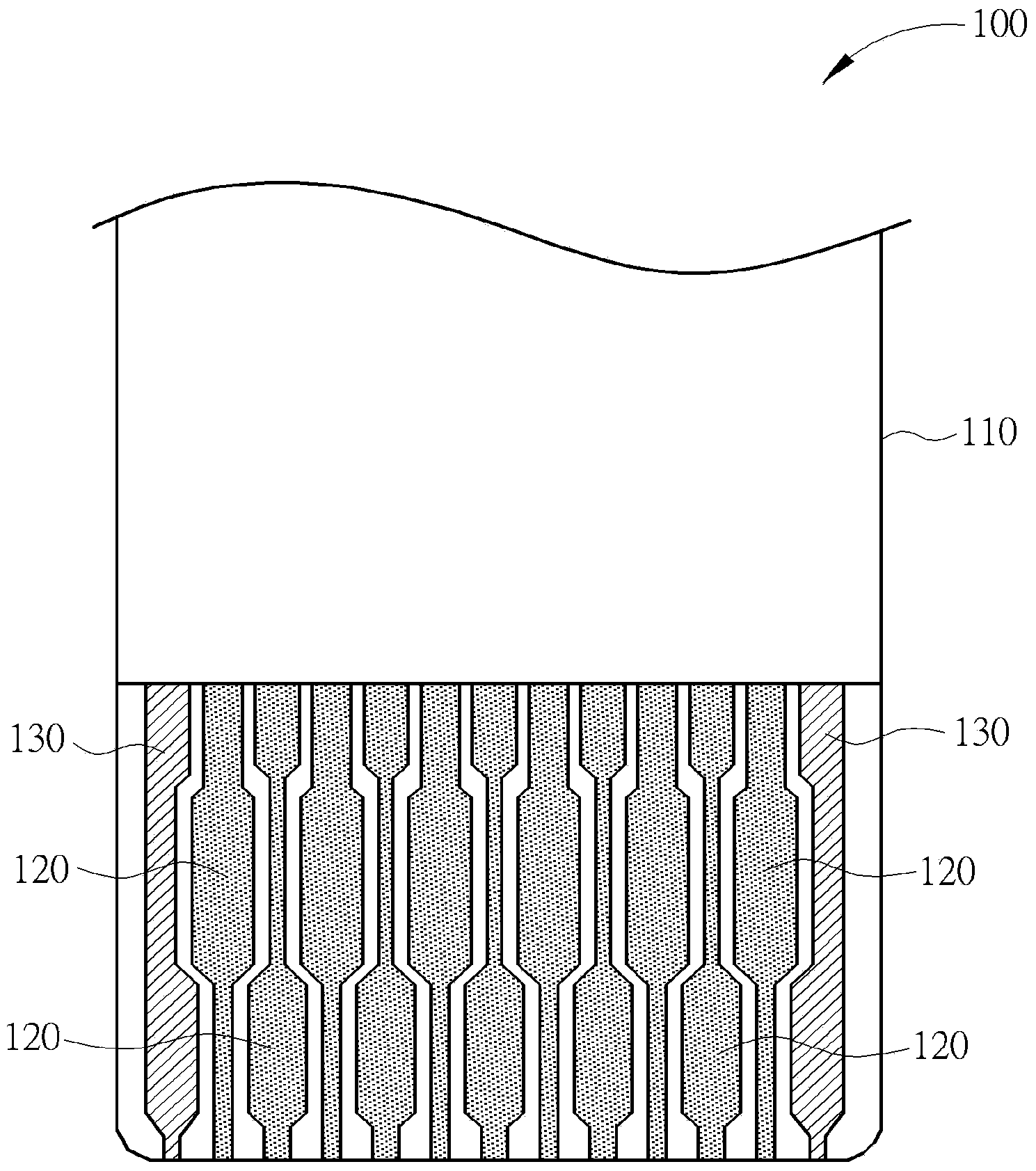
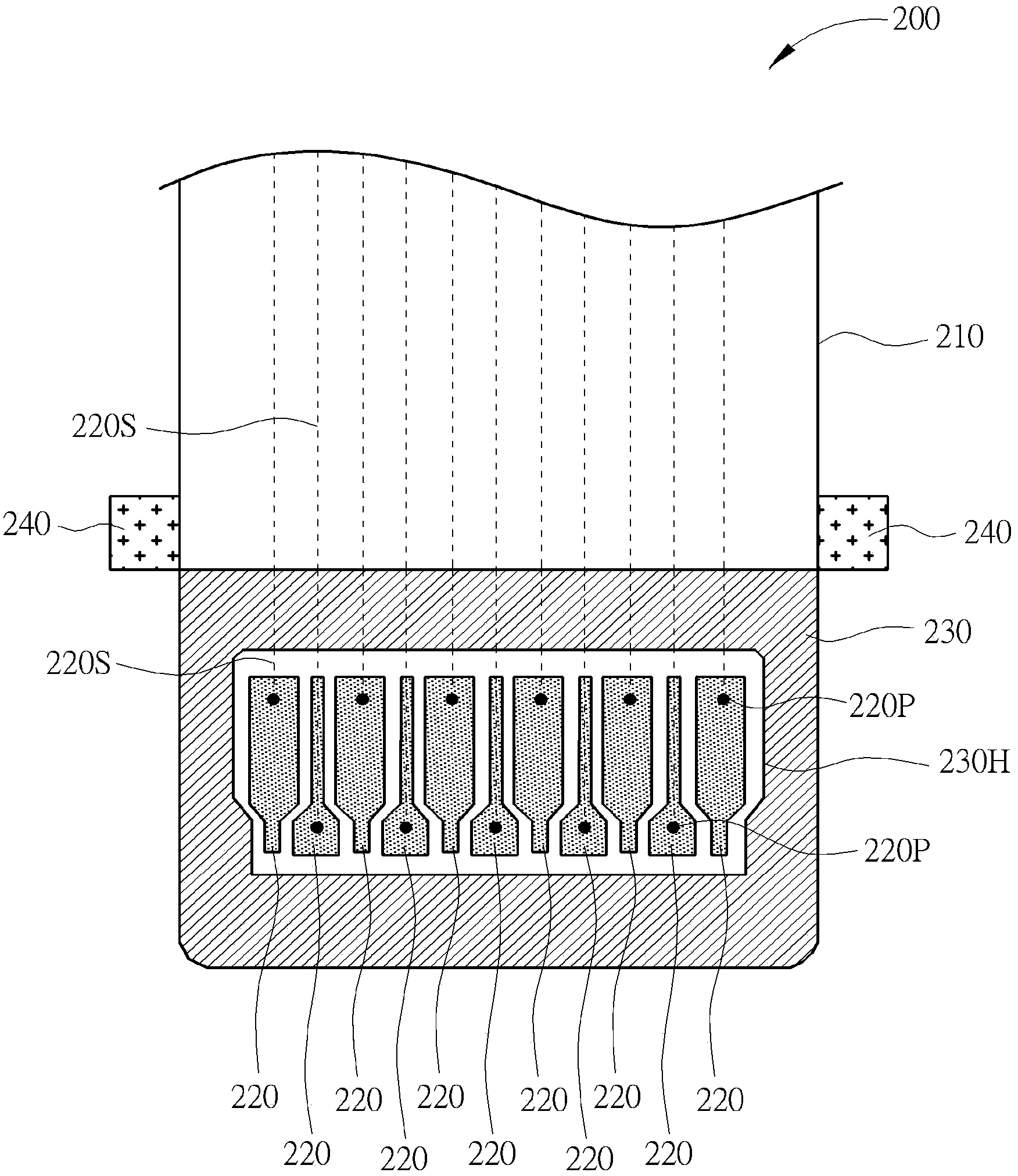
[0018] Such as figure 2 As shown, the connection structure 200 of the electronic device according to the first preferred embodiment of the present invention includes a circuit board 210 , a plurality of conductive contact pads 220 and a conductive pattern 230 . The conductive contact pad 220 and the conductive pattern 230 are disposed on the circuit board 210 . The circuit board 210 of the present invention may include a flexible circuit board, a rigid circuit board or a circuit board formed of other suitable materials. The conductive contact pads 220 are electrically separated from each other, and the conductive pattern 230 is electrically separated from the cond...


PUM


Abstract

A connection structure of an electronic device includes a circuit board, a plurality of conductive contact pads and a conductive pattern. The conductive contact pads and the conductive pattern are disposed on the circuit board. The conductive contact pads are electrically insulated from one another. The conductive pattern is electrically insulated from the conductive contact pads. The conductive pattern is disposed on at least three sides of the conductive contact pads so as to generate an electrostatic discharge protection effect for the conductive contact pads.

Description

technical field [0001] The invention relates to a connection structure of an electronic device, in particular to a connection structure with a conductive pattern surrounding a conductive contact pad on all sides to form an electrostatic protection effect. Background technique [0002] Such as figure 1 As shown, in a general ZIP-connector (ZIP-connector) 100 of a flexible printed circuit (FPC), conductive contact pads 120 (also called golden fingers) are arranged side by side on the circuit board 110 . The conductive contact pad 120 on the card insertion end 100 is used for inserting into a connector (not shown in the figure) to contact it to form an electrical connection. On the circuit board 110 , the conductive contact pad 120 is connected to, for example, an integrated circuit (IC, not shown in the figure). Therefore, when the conductive contact pad 120 is attacked by static electricity, the IC will be directly damaged and cannot function normally. Since the electricall...

Claims


Application Information

Patent Timeline
Patent Type & Authority Applications(China)
IPC IPC(8): H05K1/11H05F3/02
CPCH01R12/714H05F3/02H05K1/0259H05F3/00H01R12/7005H01R12/775H01R13/648H05K1/111H05K1/113H05K2201/09354H05K2201/09409H05K2201/09445H05K2201/097H01R13/6485
Inventor 林荣松李炫运纪品颢林志远林明传
Owner WINTEK CORP
Why Eureka
Try Eureka