Shallow-trench isolation structure and forming method thereof

A technology of isolation structure and shallow trench, which is used in the manufacture of electrical components, electrical solid-state devices, semiconductor/solid-state devices, etc.

Inactive Publication Date: 2015-02-11
SEMICONDUCTOR MANUFACTURING INTERNATIONAL (BEIJING) CORP +1
View PDF7 Cites 6 Cited by
  • Summary
  • Abstract
  • Description
  • Claims
  • Application Information

AI Technical Summary

Problems solved by technology

[0006] The isolation effect of the shallow trench isolation structure formed by the existing technology needs to be further improved

Method used


Image

  • Shallow-trench isolation structure and forming method thereof
  • Shallow-trench isolation structure and forming method thereof
  • Shallow-trench isolation structure and forming method thereof

Examples


Embodiment Construction

[0029] As mentioned in the background art, the isolation effect of the existing shallow trench isolation structure needs to be further improved.

[0030] Research has found that the shallow trench isolation structure formed in the prior art will generate leakage when the chip has a relatively high operating voltage, resulting in reduced circuit reliability and chip failure.

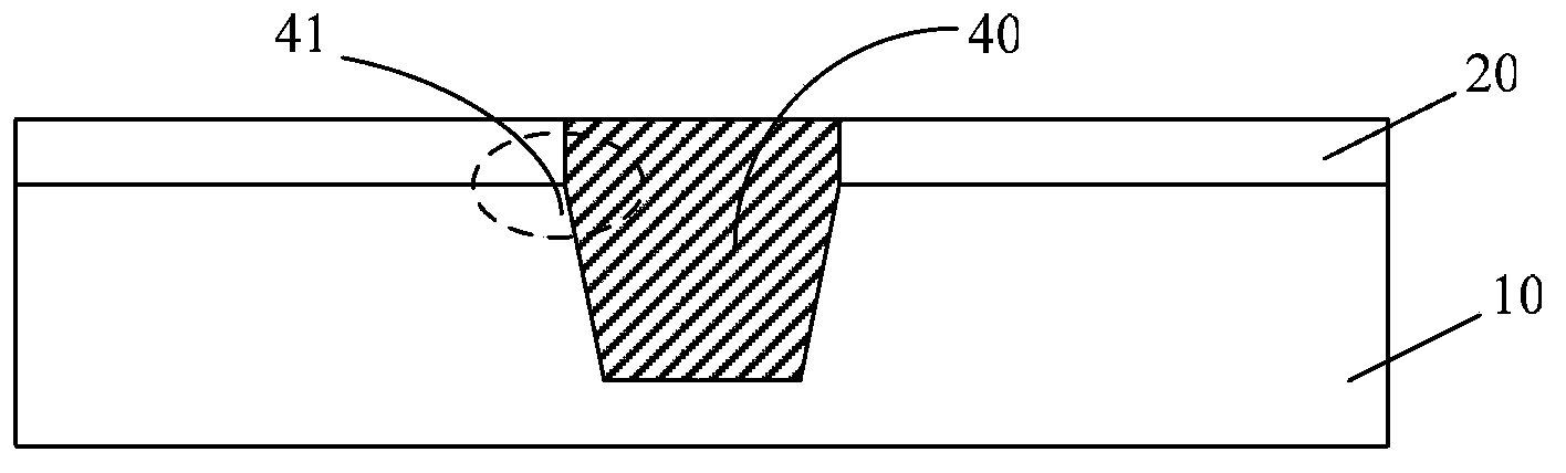
[0031] Further, research has found that under high-voltage environments, leakage is likely to occur mainly at the top corners where the semiconductor substrate and the shallow trench isolation structure are connected. Please refer to figure 2 , the angle of the vertex 41 where the semiconductor substrate 10 meets the shallow trench isolation structure 40 is relatively sharp, and in the case of a high voltage, the electric field density at the position of the vertex is relatively large, and electric leakage etc. are likely to occur phenomenon, and because the angle of the vertex 41 is relatively sharp an...


PUM


Abstract

Semiconductor devices and fabrication methods are disclosed. A mask layer having an opening is formed on a semiconductor substrate. The semiconductor substrate is etched along the opening of the mask layer to form a trench therein. The mask layer is laterally etched from the opening of the mask layer along a top surface of the semiconductor substrate to expose a surface portion of the semiconductor substrate on each side of the opening. A liner oxide layer is formed by a thermal oxidation process on interior surface of the trench and on the exposed surface portion of the semiconductor substrate. The thermal oxidation process is controlled such that an upper corner between the top surface of the semiconductor substrate and the trench is rounded after the liner oxide layer is formed. An insulation layer is formed on the liner oxide layer and fills the trench.

Description

technical field [0001] The invention relates to the technical field of semiconductors, in particular to a shallow trench isolation structure and a forming method thereof. Background technique [0002] Submicron and smaller feature sizes are one of the key technologies for next-generation VLSI and VLSI of semiconductor devices. The continuous shrinking of the size puts forward higher requirements on the formation process of semiconductors, and the formation of high-quality gate patterns and shallow trench isolation structures (STI) is the key to the development of integrated circuits. The isolation effect of the shallow trench isolation structure (STI) is very important for the reliability of the chip. [0003] Figure 1 to Figure 2 Schematic diagram of forming a shallow trench isolation structure (STI) for the prior art. [0004] Please refer to figure 1 A mask layer 20 having an opening is formed on the surface of the semiconductor substrate 10, a part of the semiconduc...

Claims


Application Information

Patent Timeline
Patent Type & Authority Applications(China)
IPC IPC(8): H01L21/762H01L27/04
CPCH01L29/0649H01L21/76235H01L21/76224
Inventor 蒲贤勇陈轶群陈宗高
Owner SEMICONDUCTOR MANUFACTURING INTERNATIONAL (BEIJING) CORP
Why Eureka
Try Eureka