Display device and method of manufacturing same

a liquid crystal display and display device technology, applied in optics, instruments, electrical appliances, etc., can solve the problems of increasing the susceptibility of the image displayed in the liquid crystal display device to display unevenness, increasing the likelihood of image shadowing, and increasing the load on the common signal line. , to achieve the effect of preventing a decrease in display quality in the display device, shortening the length of the common signal line, and reducing the risk of image shadowing

Active Publication Date: 2013-10-10
SHARP KK
View PDF12 Cites 2 Cited by
  • Summary
  • Abstract
  • Description
  • Claims
  • Application Information

AI Technical Summary

Benefits of technology

[0075]According to the first aspect, a signal wiring line that supplies a prescribed signal is formed in an open region provided corresponding to an unused output terminal section where a plurality of unused circuit output terminals included in the first driver circuit are collectively disposed. In such a case, by adjusting the position and number of unused output terminal sections, it is possible to adjust the width and length of the signal wiring line to optimal values, and to supply the prescribed signal to a desired position. Thus, it is possible to prevent a decrease in display quality in the display device.
[0076]According to the second aspect, the open region is provided in a position in the driver circuit mounting region corresponding to the unused output terminal section of the first driver circuit. The common signal line is connected to the common transfer electrode so as to pass through the open region. It is thus possible to shorten the length of the common signal line, and to position the common transfer electrode in a desired location. In this manner, variation in common signal lag for each position on the common electrode can be mitigated, thus reducing display unevenness in the image. The width of the open region is also increased, allowing the width of the common signal line to also be increased. As a result, the load on the common signal line is decreased, and thus, shadowing in the image can be reduced.
[0077]According to the third aspect, it is possible to supply a common signal to the common electrode from an external source by providing the substrate connecting region, and thus, there is no need to generate a common signal in the first driver circuit. As a result, the first driver circuit can be made smaller, thus allowing the display device to be miniaturized.
[0078]According to the fourth aspect, the common signal supplied to the common transfer electrode is generated in the common signal generating part in the first driver circuit, and thus, it is possible to shorten the length of the common signal line. As a result, the load on the common signal line is decreased, and thus, shadowing can be reduced.
[0079]According to the fifth aspect, the plurality of unused circuit output terminals are collectively formed in the boundary between the source signal output part and the gate signal output part of the one-chip driver. In this case, in the unused output terminal section, the unused circuit output terminals of not only the source signal output part, but also the gate signal output part are gathered, and thus, the unused output terminal section is widened. Thus, the resistance of the common signal line can be reduced, and therefore, display unevenness and shadowing can be mitigated.
[0080]According to the sixth aspect, the unused output terminal section of the first driver circuit is provided in the center, and thus, the open region where the common signal line is formed is formed in the center of the driver circuit mounting region. As a result, it is possible to dispose the common transfer electrode in the center of the frame region. Thus, it is possible to increase the pitch between lead-out lines connected to the output terminals of the driver circuit mounting region, thus reducing defects due to short-circuiting in the lead-out lines.

Problems solved by technology

As a result, the lag of the common signal varies depending on the position on the common electrode, which increases the susceptibility of the image displayed in the liquid crystal display device to display unevenness.
Also, the load on the common signal line becomes high, increasing the likelihood of shadowing in the image.
Liquid crystal display devices with a large display are particularly susceptible to these phenomena.

Method used


Image

  • Display device and method of manufacturing same
  • Display device and method of manufacturing same
  • Display device and method of manufacturing same

Examples


embodiment 1

1. Embodiment 1

[0122]

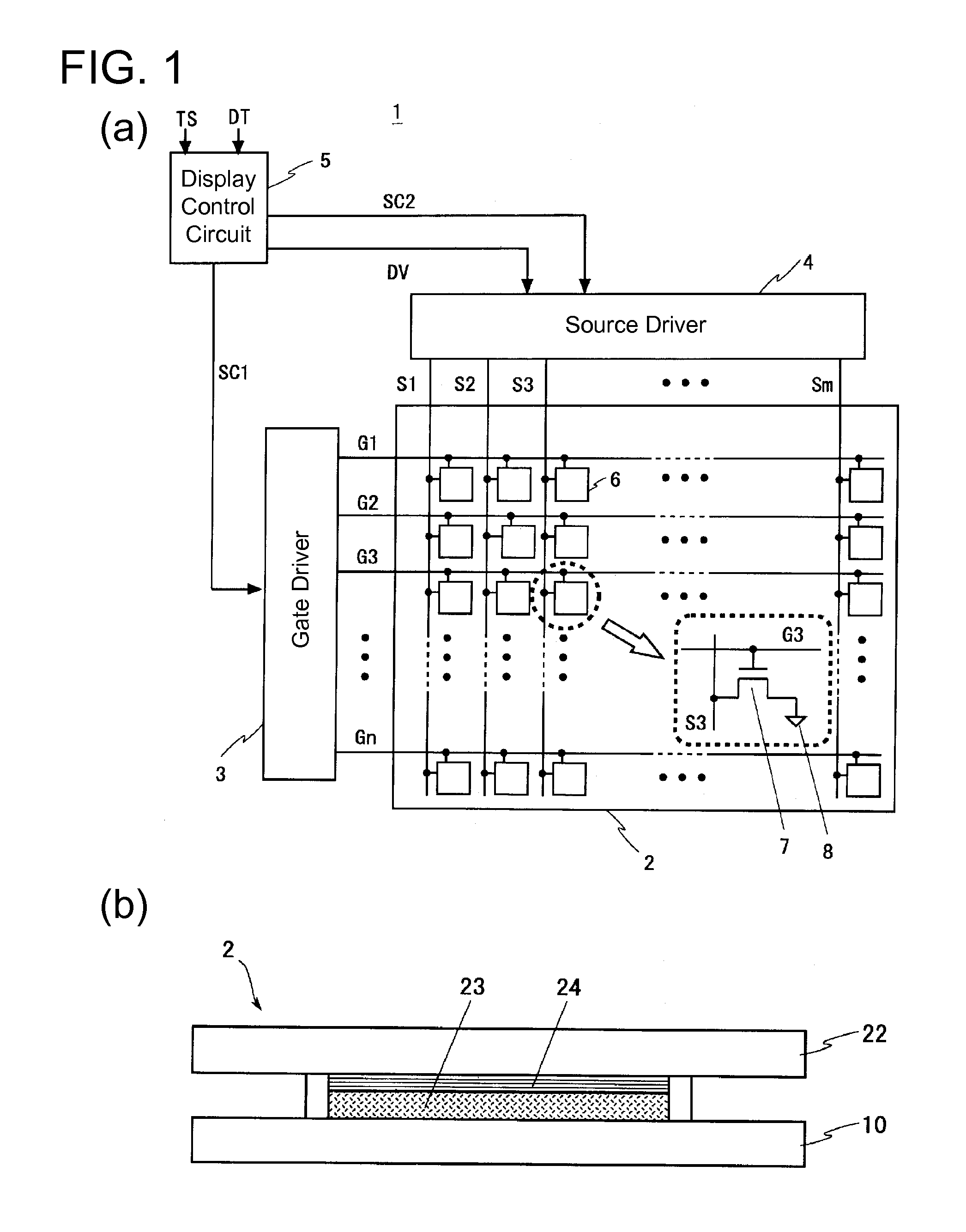
[0123]FIG. 1(a) is a block diagram that shows a configuration of an active matrix liquid crystal display device 1 according to Embodiment 1 of the present invention, and FIG. 1(b) is a cross-sectional view of a liquid crystal panel 2 included in the liquid crystal display device 1 shown in FIG. 1(a). As shown in FIG. 1(a), the liquid crystal display device 1 includes the liquid crystal panel 2, a gate driver 3, a source driver 4, and a display control circuit 5. The gate driver 3 and the source driver 4 are sometimes collectively referred to as “first driver circuits.” If a plurality of either the gate drivers 3 or the source drivers 4 are included in embodiments or application examples below, then these are sometimes collectively referred to as “second driver circuits.”

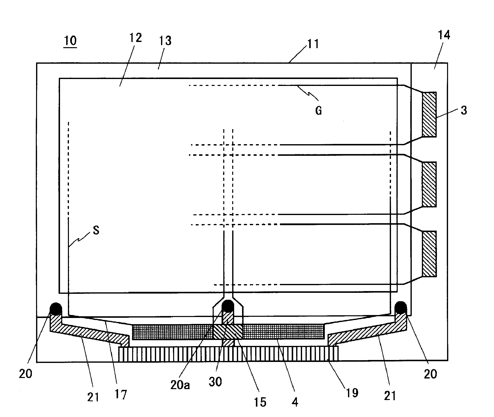
[0124]As shown in FIG. 1(b), the liquid crystal panel 2 includes a TFT substrate 10 (also referred to as a “first substrate”), an opposite substrate 22 (also referred to as a “second substrate”),...

embodiment 2

2. Embodiment 2

[0186]FIG. 20 is a drawing that shows a configuration of a TFT substrate 60 included in a liquid crystal display device 1 according to Embodiment 2 of the present invention. FIG. 21 is a magnified view of the vicinity of a source driver mounting region 25 of the TFT substrate 60 shown in FIG. 20. The configuration of the liquid crystal display device 1 of the present embodiment and the method of forming the source driver mounting region 25 are both the same as those of Embodiment 1, and therefore, descriptions thereof are omitted. Also, components that are the same as the components of the TFT substrate of Embodiment 1, or corresponding components thereof, are assigned the same reference characters with descriptions thereof omitted.

[0187]As shown in FIG. 2, in the TFT substrate 10 of Embodiment 1, the common signal was applied to the common signal lines 21 and 30 from an external source through the FPC substrate, but in the TFT substrate 60 of the present embodiment, ...

embodiment 3

3. Embodiment 3

[0190]FIG. 22 is a drawing that shows a configuration of a TFT substrate 70 included in a liquid crystal display device 1 according to Embodiment 3 of the present invention. FIG. 23 is a magnified view of the vicinity of a driver mounting region 25 of the TFT substrate 70 shown in FIG. 22. The configuration of the liquid crystal display device 1 of the present embodiment and the method of forming the driver mounting region 25 are both the same as those of Embodiment 1, and therefore, descriptions thereof are omitted. Also, components that are the same as the components of the TFT substrate 10 of Embodiment 1, or corresponding components thereof, are assigned the same reference characters with descriptions thereof omitted.

[0191]As shown in FIG. 22, in an element region 14 of the TFT substrate, a one-chip driver 9 is mounted, the one-chip driver 9 being constituted of a source signal output part 9a, and gate signal output parts 9b that sandwich the source signal output ...


PUM

PropertyMeasurementUnit
thicknessaaaaaaaaaa
thicknessaaaaaaaaaa
thicknessaaaaaaaaaa

Abstract

Provided are a display device and a method of manufacturing same, whereby deterioration in image display quality due to display unevenness or shadowing is avoided. An open region is disposed in a source driver mounting region in a position thereof that corresponds to a remaining output region 15 of a source driver 4. Next, a common signal line 30, which connects an FPC connecting region 19 to a common transfer electrode 20a, is formed passing through the open region. It is thus possible to shorten the length of the common signal line 30, and to position the common transfer electrode 20a in a desired location. Consequently, variation in the common signal rounding for each position on a common electrode is mitigated, making it possible to minimize image display unevenness. The width of the open region is also increased, allowing the width of the common signal line 30 to also be increased. Consequently, the load on the common signal line 30 can be reduced.

Description

TECHNICAL FIELD[0001]The present invention relates to a display device and a method for manufacturing the same, and particularly, to an active matrix liquid crystal display device having wiring lines for supplying a common signal to common transfer electrodes, and a method for manufacturing the same.BACKGROUND ART[0002]A liquid crystal display device includes a substrate (hereinafter referred to as a “TFT substrate”) on which a plurality of pixels each including a switching element constituted of a thin film transistor (hereinafter referred to as a “TFT”) are formed, an opposite substrate disposed opposite to the TFT substrate, and a liquid crystal layer interposed between these substrates. Liquid crystal display devices display images by controlling the light transmittance through liquid crystal by applying a voltage corresponding to an image signal (hereinafter referred to as a “signal voltage”) to a pixel electrode formed for each pixel, and applying a common voltage (also referr...

Claims


Application Information

Patent Timeline
Patent Type & Authority Applications(United States)
IPC IPC(8): G02F1/1343
CPCG02F1/1345G02F2001/13456G02F1/13458G02F1/13439G02F1/13456G02F1/136286
Inventor OGASAWARA, ISAOYOSHIDA, MASAHIRO
Owner SHARP KK
Why Eureka
Try Eureka