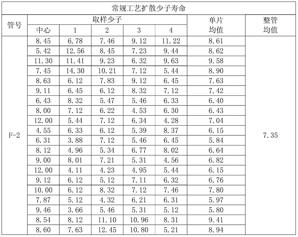
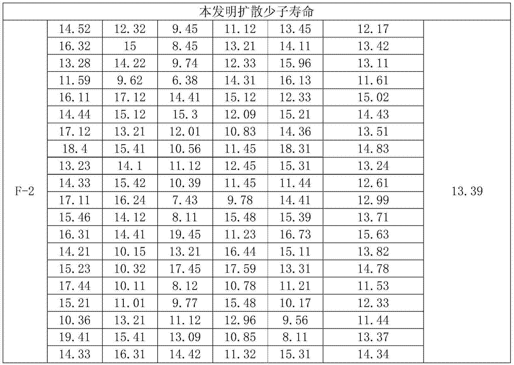
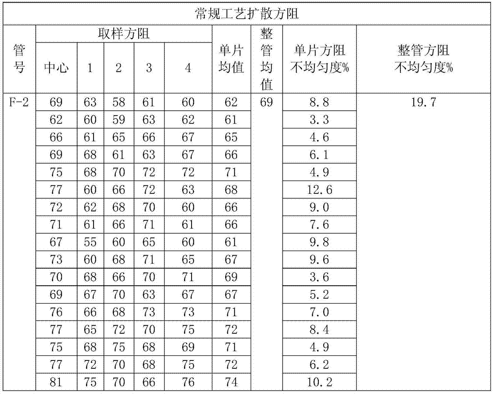
Phosphorus gettering process of silicon chips
A phosphorus gettering and silicon wafer technology, applied in sustainable manufacturing/processing, photovoltaic power generation, electrical components, etc., can solve problems affecting the photoelectric conversion efficiency of solar cells, etc., to improve short-wave response, improve uniformity, and improve phosphorus absorption The effect of miscellaneous craftsmanship
- Summary
- Abstract
- Description
- Claims
- Application Information
AI Technical Summary
Problems solved by technology
Method used
Image
Examples
Embodiment 1
[0025] A silicon wafer phosphorus gettering process, the steps are:
[0026] (1) Deposition: put the silicon chip with the suede surface into the diffusion furnace, feed nitrogen, phosphorus oxychloride and oxygen, and heat up for diffusion; this process is divided into three stages (divided into eleven steps in total), each The step time, temperature and the amount of various gases are introduced in detail as follows:
[0027] The first diffusion stage (a~e):
[0028] a. The first step of diffusion: the diffusion time is 10s, the temperature at the furnace mouth is 835°C, the temperature in the furnace is 800°C, the temperature at the end of the furnace is 800°C, the amount of nitrogen gas is 13000mL, and the input of phosphorus oxychloride and oxygen The volume is 0mL;
[0029] b. The second step of diffusion: the diffusion time is 600s, the temperature of the furnace mouth is 800°C, the temperature in the furnace is 800°C, the temperature of the furnace tail is 800°C, the...
Embodiment 2
[0043] A silicon wafer phosphorus gettering process, the steps are:
[0044] (1) Deposition: put the silicon chip with the suede surface into the diffusion furnace, feed nitrogen, phosphorus oxychloride and oxygen, and heat up for diffusion; this process is divided into three stages (divided into eleven steps in total), each The step time, temperature and the amount of various gases are introduced in detail as follows:
[0045] The first diffusion stage (a~e):
[0046] a. The first step of diffusion: the diffusion time is 30s, the temperature at the furnace mouth is 855°C, the temperature in the furnace is 820°C, the temperature at the end of the furnace is 810°C, the amount of nitrogen gas is 15000mL, phosphorus oxychloride and oxygen are introduced The volume is 0mL;
[0047] b. The second step of diffusion: the diffusion time is 800s, the temperature at the furnace mouth is 850°C, the temperature in the furnace is 830°C, the temperature at the end of the furnace is 810°C,...
Embodiment 3
[0061] A silicon wafer phosphorus gettering process, the steps are:
[0062] (1) Deposition: put the silicon chip with the suede surface into the diffusion furnace, feed nitrogen, phosphorus oxychloride and oxygen, and heat up for diffusion; this process is divided into three stages (divided into eleven steps in total), each The step time, temperature and the amount of various gases are introduced in detail as follows:
[0063] The first diffusion stage (a~e):
[0064] a. The first step of diffusion: the diffusion time is 30s, the temperature at the furnace mouth is 855°C, the temperature in the furnace is 820°C, the temperature at the end of the furnace is 810°C, the amount of nitrogen gas is 15000mL, phosphorus oxychloride and oxygen are introduced The volume is 0mL;
[0065] b. The second step of diffusion: the diffusion time is 800s, the temperature at the furnace mouth is 850°C, the temperature in the furnace is 830°C, the temperature at the end of the furnace is 810°C,...
PUM
 Abstract
Description
Claims
Application Information
 - R&D
- Intellectual Property
- Life Sciences
- Materials
- Tech Scout
- Unparalleled Data Quality
- Higher Quality Content
- 60% Fewer Hallucinations
Browse by: Latest US Patents, China's latest patents, Technical Efficacy Thesaurus, Application Domain, Technology Topic, Popular Technical Reports.
© 2025 PatSnap. All rights reserved.Legal|Privacy policy|Modern Slavery Act Transparency Statement|Sitemap|About US| Contact US: help@patsnap.com


