


Quick Research
Generate reliable direction feasibility study reports for your R&D in just a few steps.

Technical Q&A
Discover and master advanced knowledge NOW. Basics, ideas, possibilities, all at once.

Find Solutions
As an expert in R&D theories, this can generate solutions to your technical problems instantly.

Evaluate Feasibility
Analyze your overall solution with one click, know your potential R&D risks in advance.

Monitor Landscape
Get weekly tech updates, stay abreast of the latest tech innovations and key insights.
A kind of thin film transistor and its manufacturing method, photolithography process
A thin-film transistor and photolithography technology, which is applied in transistors, semiconductor/solid-state device manufacturing, semiconductor devices, etc., can solve the problems of complex structure and complex manufacturing process, and achieve the goal of simplifying the lithography process, reducing the manufacturing process, and reducing the manufacturing cost. Effect
- Summary
- Abstract
- Description
- Claims
- Application Information
AI Technical Summary
Problems solved by technology
Method used
Image

Examples
Embodiment 1
[0044] This embodiment provides a photolithography process, such as Figure 7 to Figure 9 shown, including the following steps:
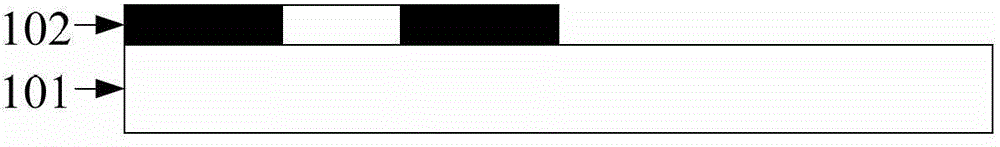
[0045] Step 1: If Figure 7 As shown, a substrate 701 is provided, and a film layer A and a film layer B are formed on one surface of the substrate 701 , wherein the film layer B is located between the substrate 701 and the film layer A.
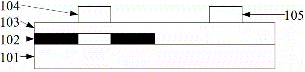
[0046] Step 2: If Figure 8 As shown, a photoresist layer 702 is formed on the surface of the film layer A, and the photoresist layer 702 can be a positive photoresist layer or a negative photoresist layer. The material of the photoresist layer 702 is not limited, and can be selected according to specific needs and process conditions.
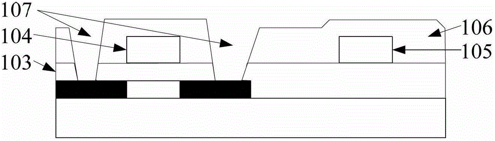
[0047] Step 3: If Figure 9 As shown, the photoresist layer 702 is exposed using a half-grayscale mask 703, wherein the half-grayscale mask 703 includes a first region 7031, a second region 7032 and a third region 7033, and The light transmittance of the first region 7031 and ...
Embodiment 2
[0064] This embodiment provides a method for manufacturing a thin film transistor, such as Figure 15 shown, including the following steps:
[0065] Step 1501: providing a substrate, for a thin film transistor, the substrate is a transparent substrate, preferably, the substrate is a glass substrate;
[0066] Step 1502: if Figure 16 As shown, silicon islands 1602 are formed on the surface of the substrate 1601 .
[0067] According to the types of thin film transistors, the types of silicon islands 1602 currently include amorphous silicon islands, polycrystalline silicon islands, and single crystal silicon islands. High efficiency, low power consumption and other advantages, so low-temperature polysilicon thin film transistors are more and more valued by flat-panel display manufacturers, and their applications in smart phone displays are becoming more and more extensive. Therefore, in this embodiment, it is preferable to take a low-temperature polysilicon thin film transisto...
Embodiment 3
[0094] This implementation provides a thin film transistor such as Figure 27 As shown, the thin film transistor is manufactured by the manufacturing method described in the second embodiment. The gate and transparent electrode of this kind of thin film transistor are completed by one photolithography process, so the whole manufacturing process of this kind of thin film transistor only needs to use four photolithography processes, the manufacturing method is simple, and the cost is low.
PUM
 Abstract
Description
Claims
Application Information
 - R&D Engineer
- R&D Manager
- IP Professional
- Industry Leading Data Capabilities
- Powerful AI technology
- Patent DNA Extraction
Browse by: Latest US Patents, China's latest patents, Technical Efficacy Thesaurus, Application Domain, Technology Topic, Popular Technical Reports.
© 2024 PatSnap. All rights reserved.Legal|Privacy policy|Modern Slavery Act Transparency Statement|Sitemap|About US| Contact US: help@patsnap.com