
Visible light communication device based on LED projection

A visible light communication and projection technology, which is applied in the field of lighting and communication, can solve the problems of not much communication research on low-power and high-density array modules, no finished products for small-pitch LED array modules, high requirements for packaging technology and technology, and meet the application requirements. Wide, small power, small size effect

Inactive Publication Date: 2015-01-07
INST OF SEMICONDUCTORS - CHINESE ACAD OF SCI
View PDF8 Cites 4 Cited by
  • Summary
  • Abstract
  • Description
  • Claims
  • Application Information

AI Technical Summary

Problems solved by technology

[0006] However, there is no small-pitch high-density LED device product that integrates the two functions of projection lighting and communication.
The reasons can be attributed to the following three points: First, the LED chip size is small and the integration level is high, so the requirements for the packaging process and technology are very high, resulting in the small-pitch LED array module is still in the research and development stage and there is no finished product
The second is that the light source in the multi-channel parallel visible light communication system mostly uses a single or several medium and high-power single-color or dual-color LEDs, and there are not many studies on the communication of low-power and high-density array modules; the third is the origin of the concept of projection lighting. It has been a long time, but the research on LED projection lighting is just in its infancy, so there is little in-depth research on the visible light system that combines high-density LED projection lighting with communication.

Method used


Image

  • Visible light communication device based on LED projection
  • Visible light communication device based on LED projection

Examples


Embodiment Construction

[0023] It should be noted that, in the drawings or descriptions of the specification, similar or identical parts all use the same figure numbers. Implementations not shown or described in the accompanying drawings are forms known to those of ordinary skill in the art. Additionally, while illustrations of parameters including particular values ​​may be provided herein, it should be understood that the parameters need not be exactly equal to the corresponding values, but rather may approximate the corresponding values ​​within acceptable error margins or design constraints. The directional terms mentioned in the embodiments, such as "upper", "lower", "front", "rear", "left", "right", etc., are only referring to the directions of the drawings. Therefore, the directional terms used are for illustration and not for limiting the protection scope of the present invention.

[0024] The visible light communication device based on LED projection in the present invention uses a highly i...


PUM


Abstract

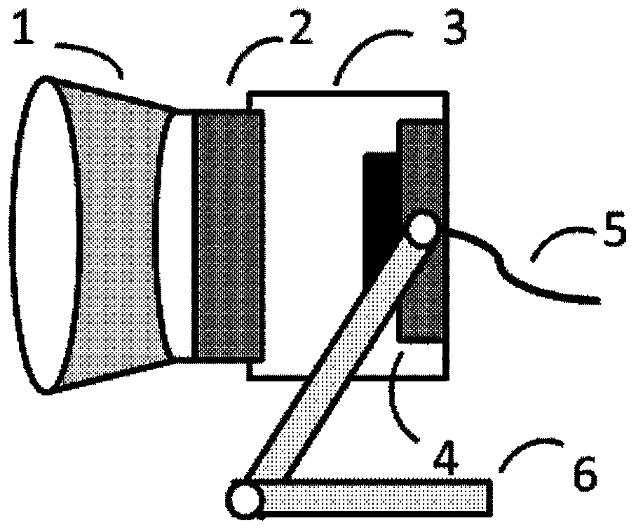
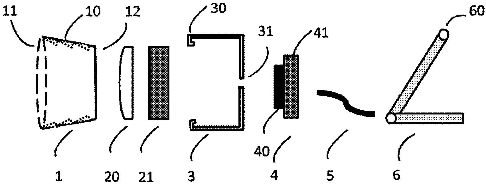
A visible light communication device based on LED projection comprises a light source module, a primary light source outer cover, an optical element device and a secondary light source outer cover. The light source module is used for emitting LED light, and is controlled by a drive circuit to achieve the illumination and communication functions at the same time. The light source module is fixed to the inner wall of the rear end of the primary light source outer cover, and the LED light convergence function is achieved. The optical element device is fixed to the front end of the primary light source outer cover, and is used for controlling the definition and size of a projection image. The secondary light source outer cover is fixed to the front end of the optical element device, and is adopted as an LED projection and illumination distance and range adjusting component. The visible light communication device has the advantages of being relatively simple in module structure, relatively small in size and large in application area and saving cost.

Description

technical field [0001] The present invention relates to the fields of illumination and communication, in particular to a visible light communication device based on LED projection. Background technique [0002] Today, when advocating energy-saving, environmentally friendly and low-carbon life, light-emitting diodes (LEDs) are more and more widely used in the fields of lighting, display and communication. Visible light communication technology based on semiconductor lighting has high bandwidth, no electromagnetic pollution, good security, low power consumption, no need for new dedicated network and frequency licenses, certain mobility, and the advantages brought by the combination with semiconductor lighting. With the advantages of energy saving and environmental protection, and with the further development of semiconductor lighting technology and the increasing popularity of semiconductor lighting, it may become the main access method of network terminals. Therefore, the po...

Claims


Application Information

Patent Timeline
IPC IPC(8): H04B10/116
Inventor 裴艳荣杨华王军喜李晋闽
Owner INST OF SEMICONDUCTORS - CHINESE ACAD OF SCI
Learn More