Film formation method of n-type In2S3 buffer layer and application of film formation method of n-type In2S3 buffer layer
A film-forming method and a buffer layer technology, which are applied in coating, metal material coating process, ion implantation plating, etc., can solve the problems of thin-film light-transmitting solar cell performance, difficulty in accurately controlling film composition, etc., and achieve conductive The effect of good characteristics and stable device performance
- Summary
- Abstract
- Description
- Claims
- Application Information
AI Technical Summary
Problems solved by technology
Method used
Image
Examples
preparation example Construction
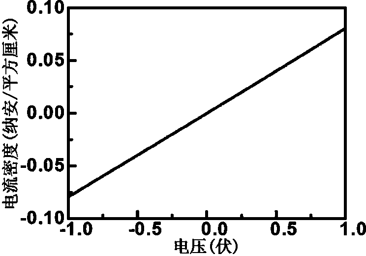
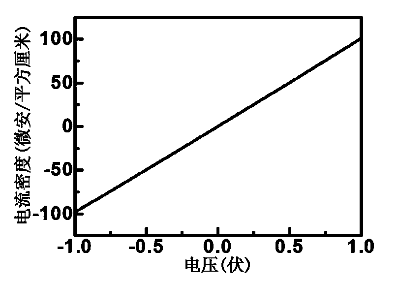
[0055] Using the n-type In of the present invention 2 S 3 The product obtained by the buffer layer method is further prepared into a solar cell, which is composed of n-In 2 S 3 The buffer layer 3 of the film and the substrate 1 made of p-Si are composed; the n-In 2 S 3 The buffer layer 3 of the film is β-In 2 S 3 Film composition. The top surface of the substrate 1 made of p-Si is made of n-In 2 S 3 The bottom surface of the buffer layer 3 of the film is connected; the material is n-In 2 S 3 The top surface of the buffer layer 3 of the film is provided with circular electrodes 4 arranged in an array with a thickness of 30-50 nm and made of metal In; on the bottom surface of the substrate 1 made of p-Si, a material The bottom electrode layer 2 of metal Ag; the n-In 2 S 3 The resistivity of the buffer layer 3 of the film is 1.00 – 5.00×10 -3 Ω·cm; the open circuit voltage of the solar cell is 0.29 V, the short circuit current is 7.7 nA, and the fill factor is 0.39.
[0056] Further...
Embodiment 1
[0061] Using glass as the substrate, soak in acetone, ethanol, and deionized water for ultrasonic cleaning for 8 minutes, take it out, and dry it in a vacuum drying oven; put In 2 S 3 The compound target is fixed on the target holder, the silicon wafer is fixed on the sample holder, the temperature of the vacuum chamber is normal temperature, and the vacuum is pumped to 5×10 -3 Below Pa, the target holder speed is 5r / min counterclockwise, the sample holder speed is clockwise 5r / min, the laser wavelength is 248nm, the pulse width is 25ns, the laser energy is 154mJ, the laser frequency is 5Hz, and the coating time is 30min. During annealing, the rapid annealing furnace is pre-evacuated to 1 Pa, then Ar gas is introduced to atmospheric pressure, and then vacuumed, vacuuming and charging are repeated 2 times, and then Ar gas is continuously introduced, maintaining the pressure at about 0.04 MPa, at 4℃ / The temperature is increased to 300°C at the speed of s, and the temperature is ma...
Embodiment 2
[0064] Using p-type silicon wafer as the substrate 1, soak in acetone, ethanol, and deionized water for ultrasonic cleaning for 8 minutes, take it out, and dry it in a vacuum drying oven; 2 S 3 The compound target is fixed on the target holder, the silicon wafer is fixed on the sample holder, the temperature of the vacuum chamber is normal temperature, and the vacuum is pumped to 5×10 -3 Below Pa, the target holder speed is 5r / min counterclockwise, the sample holder speed is 5r / min clockwise, the laser wavelength is 248nm, the pulse width is 25ns, the laser energy is 174mJ, the laser frequency is 5Hz, and the coating time is 30min. During annealing, the rapid annealing furnace is pre-evacuated to below 1Pa, then Ar gas is introduced to atmospheric pressure, vacuuming and charging are repeated twice, and then Ar gas is introduced to maintain the pressure at about 0.04 MPa, and the temperature is increased at a rate of 4°C / s. 300°C, keep this temperature for 30 minutes, then drop t...
PUM
| Property | Measurement | Unit |
|---|---|---|
| electrical resistivity | aaaaa | aaaaa |
| electrical resistivity | aaaaa | aaaaa |
| diameter | aaaaa | aaaaa |
Abstract
Description
Claims
Application Information
 - Generate Ideas
- Intellectual Property
- Life Sciences
- Materials
- Tech Scout
- Unparalleled Data Quality
- Higher Quality Content
- 60% Fewer Hallucinations
Browse by: Latest US Patents, China's latest patents, Technical Efficacy Thesaurus, Application Domain, Technology Topic, Popular Technical Reports.
© 2025 PatSnap. All rights reserved.Legal|Privacy policy|Modern Slavery Act Transparency Statement|Sitemap|About US| Contact US: help@patsnap.com


