Broadband low-consumption junior unit left-handed material based on double crosses
A double-cross type and cross-type technology, applied in the direction of electrical components, antennas, etc., can solve the problems of complex structure, large volume, large loss, etc., and achieve the effect of broadening the application field and simple processing technology.
- Summary
- Abstract
- Description
- Claims
- Application Information
AI Technical Summary
Problems solved by technology
Method used
Image
Examples
Embodiment 1
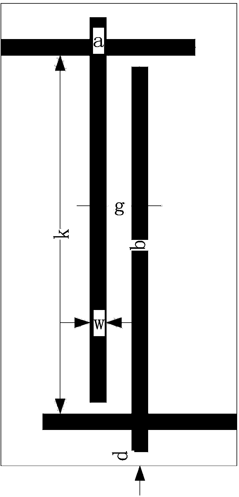
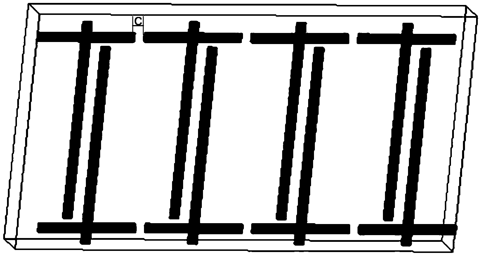
[0031] Using circuit board etching technology, a double-cross-type metal line structure unit array is etched on a certain surface of an epoxy resin PCB substrate with a thickness of 0.5mm, and the unit spacing is c=0.15mm. The length of the short horizontal line of the double-cross metal wire is a=1.4mm, the length of the long vertical line is b=2.8mm, the line width of the straight line is w=0.12mm, the horizontal distance between the two cross-shaped metal wires is g=0.18mm, the longitudinal The distance k=2.6mm, and the distance d=0.1mm between the metal wire structure and the upper and lower boundaries. Cut the etched PCB board into a size of 10.08mm × 6.35mm to obtain a single-layer double-cross type left-hand material as attached figure 2 shown.
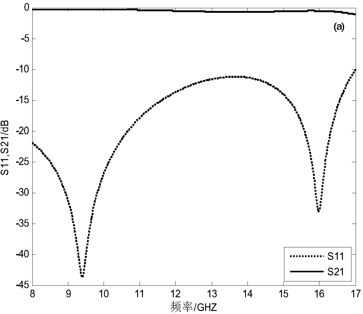
[0032] The structure was simulated using the commercial electromagnetic simulation software Ansoft HFSS. Simulation S-parameters as attached Figure 3(a) , 3(b) shown, Figure 3(a) is S 11 , S 21 It can be seen that there...
Embodiment 2
[0034]Using circuit board etching technology, a double-cross-type metal line structure unit array is etched on a certain surface of an epoxy resin PCB substrate with a thickness of 0.7mm, and the unit spacing is c=0.25mm. The length of the short horizontal line of the double-cross metal wire a=2.3mm, the length of the long vertical line b=3.1mm, the line width of the straight line w=0.15mm, the horizontal distance between the two cross-shaped metal wires g=0.15mm, the longitudinal The distance k=3.8mm, and the distance d=0.05mm between the metal wire structure and the upper and lower boundaries. Cut the etched PCB board into a size of 16.95mm × 8.24mm to obtain a single-layer double-cross type left-hand material as attached Figure 5 shown.
Embodiment 3
[0036] Using circuit board etching technology, a double-cross-type metal line structure unit array is etched on a certain surface of an epoxy resin PCB substrate with a thickness of 1.0mm, and the unit spacing is c=0.3mm. The length of the short horizontal line of the double-cross metal wire a=4.0mm, the length of the long vertical line b=5.5mm, the line width of the straight line w=0.2mm, the horizontal distance between the two cross-shaped metal wires g=0.1mm, the longitudinal The distance k=4.6mm, and the distance d=0mm between the metal wire structure and the upper and lower boundaries. Cut the etched PCB board into a size of 7.19mm × 17.2mm to obtain a single-layer double-cross type left-hand material as attached. Image 6 shown.
PUM
| Property | Measurement | Unit |
|---|---|---|
| Length | aaaaa | aaaaa |
| Length | aaaaa | aaaaa |
| Length | aaaaa | aaaaa |
Abstract
Description
Claims
Application Information
 - R&D
- Intellectual Property
- Life Sciences
- Materials
- Tech Scout
- Unparalleled Data Quality
- Higher Quality Content
- 60% Fewer Hallucinations
Browse by: Latest US Patents, China's latest patents, Technical Efficacy Thesaurus, Application Domain, Technology Topic, Popular Technical Reports.
© 2025 PatSnap. All rights reserved.Legal|Privacy policy|Modern Slavery Act Transparency Statement|Sitemap|About US| Contact US: help@patsnap.com


