
Molecular sensor based on virtual buried nanowire

A molecular and surface-sensing technology, applied in instruments, analytical materials, scientific instruments, etc., can solve the problems of commercial gas sensors being infeasible, cost increasing, and incapable of adapting to high-capacity manufacturing

Active Publication Date: 2014-12-10
RAMOT AT TEL AVIV UNIV LTD
View PDF13 Cites 2 Cited by
  • Summary
  • Abstract
  • Description
  • Claims
  • Application Information

AI Technical Summary

Problems solved by technology

However, the fabrication of commercial gas sensors based on such nanowires is currently not feasible because the fabrication of these structures using, for example, the VLS method is not amenable to high-volume manufacturing (HVM)
Alternatively, high-volume CMOS fabrication of nanowires could be realized in the future, but at the same time the cost increases substantially, even by several orders of magnitude

Method used


Image

  • Molecular sensor based on virtual buried nanowire
  • Molecular sensor based on virtual buried nanowire
  • Molecular sensor based on virtual buried nanowire

Examples


example

[0110] Reference is now made to the following examples, which together with the foregoing description illustrate some embodiments of the invention in a non-limiting manner.

[0111] The universal silicon configuration of virtual embedded nanowire gas sensors is experimentally confirmed using bioassays. In this experiment, the thickness of the SOI layer is 260nm, which has 1.6x10 14 cm -3 doped with boron so that the SOI layer has a resistivity of 13 to 22 Ωcm. The thickness of the buried oxide is 1 μm. SiO 2 The thickness of the gate dielectric is 5 nm. The active region, including the wider portions adjacent to the source and drain regions, is doped with a 1.6x10 17 cm -3 range of arsenic. The source and drain regions are doped with a 5x10 19 cm -3 range of arsenic, and the lateral gate region is doped with a 5x10 19 cm -3 range of boron. The distance from the source region to the drain region is 10 μm, and the length of the active region defined as the length of ...


PUM

PropertyMeasurementUnit
widthaaaaaaaaaa
thicknessaaaaaaaaaa
thicknessaaaaaaaaaa

Abstract

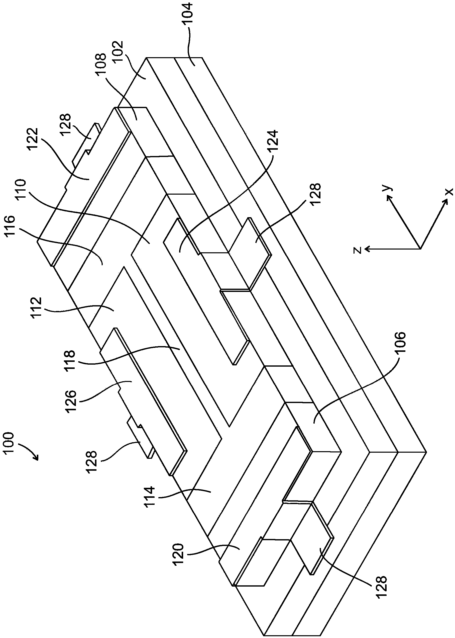
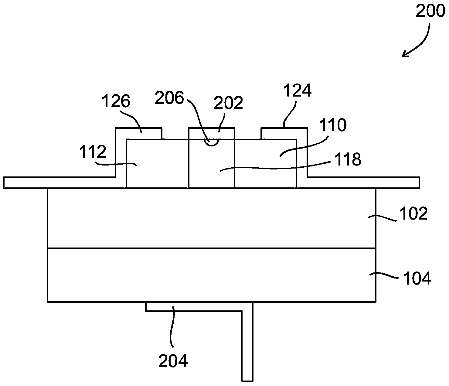
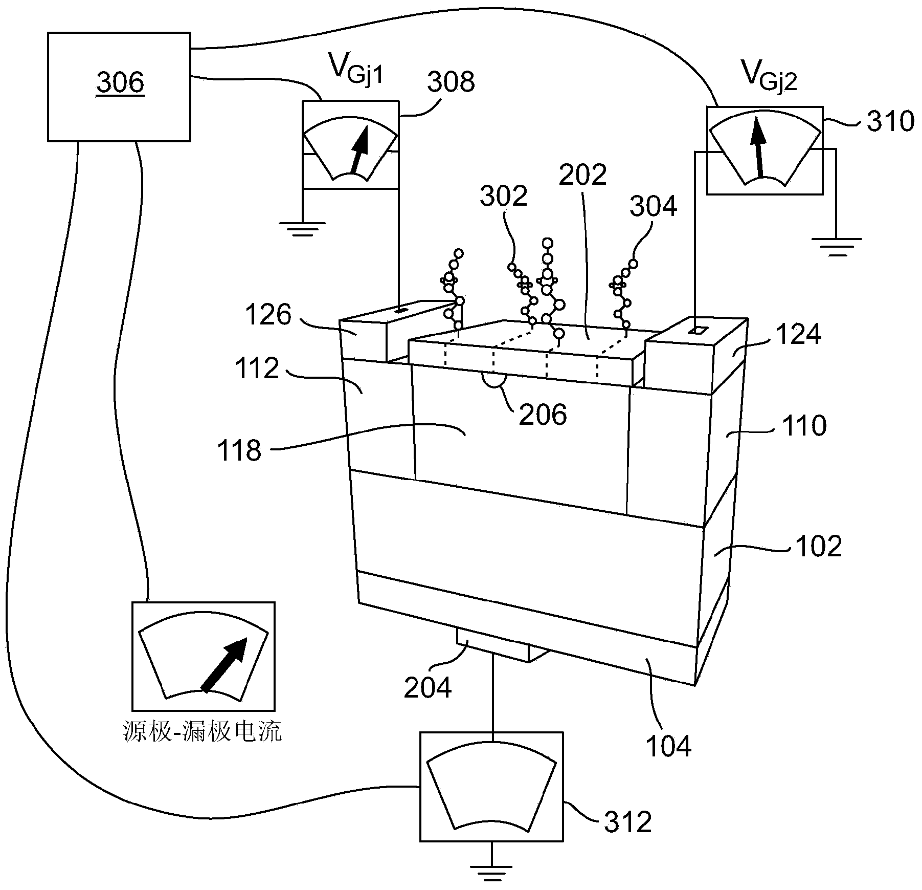
The present invention provides a method and a system based on a multi-gate filed effect transistor for sensing molecules in a gas or liquid sample. The said FET transistor comprises dual gate lateral electrodes (and optionally a back gate electrode) located on the two sides of an active region, and a sensing surface on top of the said active region. Appling voltages to the lateral gate electrodes, creates a conductive channel in the active region, wherein the width and the lateral position of the said channel can be controlled. Enhanced sensing sensitivity is achieved by measuring the channels conductivity at a plurality of positions in the lateral direction. The use of an array of the said FTE for electronic nose is also disclosed.

Description

[0001] Related applications [0002] This application asserts the benefit under 35 U.S.C. §119(e) of U.S. Provisional Patent Application No. 61 / 604,041, filed February 28, 2012, the contents of which are hereby incorporated by reference as if reproduced in their entirety . technical field [0003] In some embodiments of the invention, the invention relates to a semiconductor chemical sensor, and more particularly, but not exclusively, to a field effect transistor based gas sensor. Background technique [0004] Commercially available gas sensors include infrared sensors, toxic gas sensors, and catalytic combustion sensors, all of which are sold by City Technology, Ltd.; and by FIS, Inc. .) metal oxide gas detectors for sale. Sensors sold by City Tech, for example, are described at www.citytech.com, and sensors sold by Figaro, for example, are described at www.figarosensor.com. Gas sensors that could be less expensive to manufacture and / or had greater sensitivity and / or gr...

Claims


Application Information

Patent Timeline
Patent Type & Authority Applications(China)
IPC IPC(8): G01N27/414H01L29/772
CPCG01N27/4146G01N33/54373G01N33/551G01N27/12G01N27/30G01N27/4145H01L21/22H01L21/324
Inventor 吉尔·沙莱夫约西·罗森瓦克斯
Owner RAMOT AT TEL AVIV UNIV LTD
Learn More