
Light-emitting diode packaging structure

一种发光二极管、封装结构的技术,应用在电气元件、电固体器件、电路等方向,能够解决发光二极管光源易有眩光、出光角度有限、无法具有等问题

Active Publication Date: 2017-04-05
NICHIA CORP
View PDF5 Cites 0 Cited by
  • Summary
  • Abstract
  • Description
  • Claims
  • Application Information

AI Technical Summary

Problems solved by technology

[0003] The light emitting diode light source is a directional light source, so the direct light area in front of the light emitting diode light source usually has high brightness, which leads to the problem of glare easily caused by the light emitting diode light source
Generally speaking, in the LED packaging structure, the encapsulant covering the LED chip is in the shape of a lens. However, the lens-shaped encapsulant has a limited light emitting angle and cannot reach the surface with a large light emitting angle. The efficacy of the light source

Method used


Image

  • Light-emitting diode packaging structure
  • Light-emitting diode packaging structure
  • Light-emitting diode packaging structure

Examples


Embodiment Construction

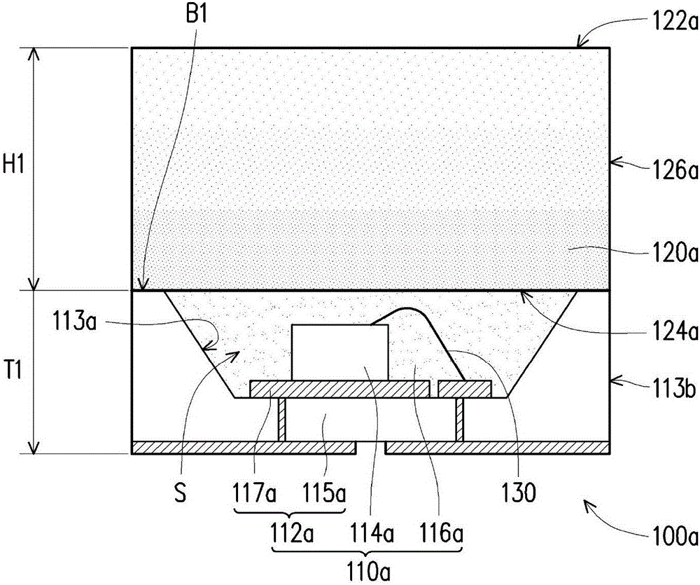
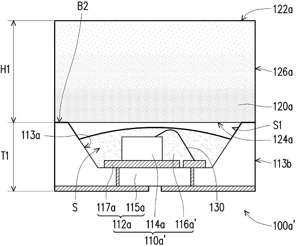
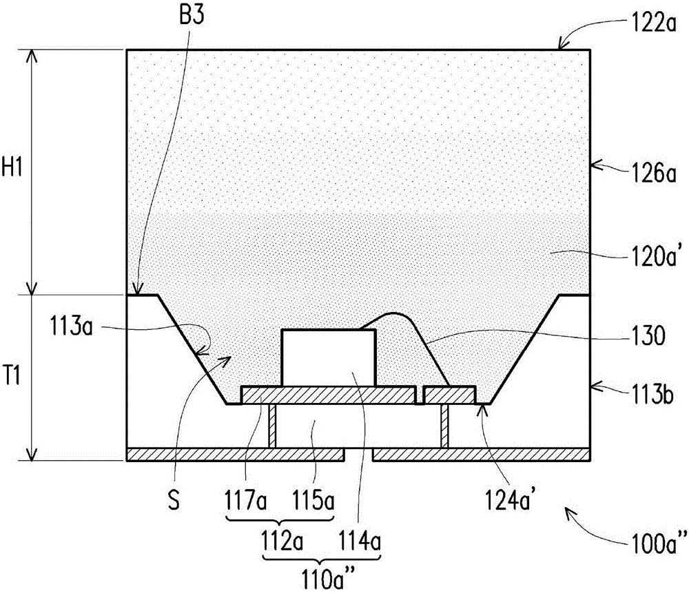
[0053] Figure 1A It is a schematic cross-sectional view of a light emitting diode packaging structure according to an embodiment of the present invention. Please refer to Figure 1A , in this embodiment, the LED packaging structure 100a includes a light emitting element 110a and a transparent packaging compound 120a. The light emitting element 110a has an upper surface B1. The transparent encapsulant 120a is disposed on the light emitting element 110a and covers the upper surface B1. The transparent encapsulant 120a has a top surface 122a and a bottom surface 124a opposite to each other and a first peripheral surface 126a connecting the top surface 122a and the bottom surface 124a. In particular, the surface area of ​​the first peripheral surface 126a of the transparent encapsulant 120a is greater than or equal to four times the horizontal projected area of ​​the upper surface B1.

[0054] In detail, in this embodiment, the light emitting element 110a includes a carrier 112...


PUM


Abstract

The invention provides an LED packaging structure which comprises a light emitting component and a transparent packaging adhesive body. The light emitting component includes an upper surface, and the transparent packaging adhesive body is arranged on the light emitting component and covers the upper surface. The transparent packaging adhesive body includes a top surface, a bottom surface and a first peripheral surface, wherein the top surface is opposite to the bottom surface, and the top surface is connected with the bottom surface via the first peripheral surface. The area of the first peripheral surface is four times the horizontal projection area of the upper surface or more.

Description

technical field [0001] The present invention relates to a semiconductor package structure, and in particular to a light emitting diode package structure. Background technique [0002] With the advancement of optoelectronic technology, the technology of light-emitting diodes (Light-emitting diodes, LEDs), which are used to replace traditional incandescent bulbs and fluorescent tubes, is gradually becoming mature. Because light-emitting diodes have the advantages of low power consumption, small size, non-thermoluminescence, and environmental protection, their application fields are gradually being promoted. [0003] The light emitting diode light source is a directional light source, so the direct light area located in front of the light emitting diode light source usually has relatively high brightness, which leads to the problem that the light emitting diode light source is prone to glare. Generally speaking, in the LED packaging structure, the encapsulant covering the LED ...

Claims


Application Information

Patent Timeline
Patent Type & Authority Patents(China)
IPC IPC(8): H01L33/48H01L33/54H01L33/58
CPCH01L2224/48091H01L2224/48227H01L2924/00014
Inventor 李允立苏柏仁
Owner NICHIA CORP
Learn More