Light emitting diode encapsulation structure

A technology of light-emitting diodes and packaging structures, which is applied in the direction of electrical components, electric solid-state devices, circuits, etc., and can solve problems such as inability to have light-emitting diode light sources that are prone to glare and limited light output angles

Inactive Publication Date: 2016-12-21
GENESIS PHOTONICS
View PDF3 Cites 0 Cited by
  • Summary
  • Abstract
  • Description
  • Claims
  • Application Information

AI Technical Summary

Problems solved by technology

[0005] The light emitting diode light source is a directional light source, so the direct light area in front of the light emitting diode light source usually has high brightness, which leads to the problem of glare easily caused by the light emitting diode light source
Generally speaking, in the LED packaging structure, the encapsulant covering the LED chip is in the shape of a lens. However, the lens-shaped encapsulant has a limited light emitting angle and cannot reach the surface with a large light emitting angle. The efficacy of the light source

Method used


Image

  • Light emitting diode encapsulation structure
  • Light emitting diode encapsulation structure
  • Light emitting diode encapsulation structure

Examples


Embodiment Construction

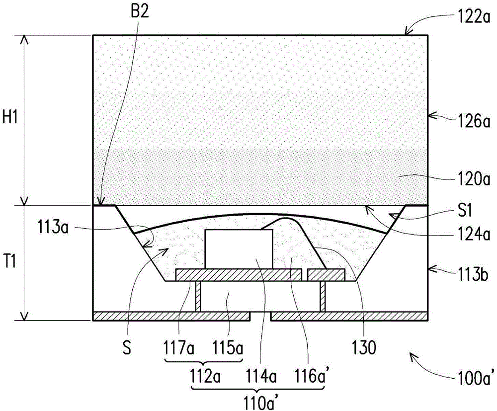
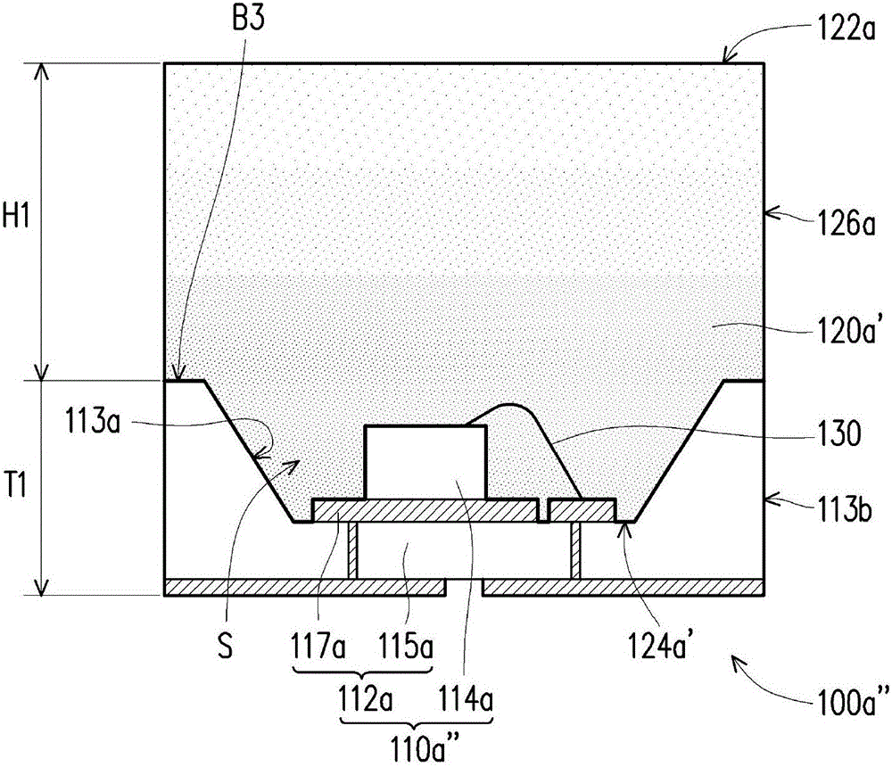
[0055] Figure 1A It is a schematic cross-sectional view of a light emitting diode packaging structure according to an embodiment of the present invention. Please refer to Figure 1A , in this embodiment, the LED packaging structure 100a includes a light emitting element 110a and a transparent packaging compound 120a. The light emitting element 110a has an upper surface B1. The transparent encapsulant 120a is disposed on the light emitting element 110a and covers the upper surface B1. The transparent encapsulant 120a has a top surface 122a and a bottom surface 124a opposite to each other and a first peripheral surface 126a connecting the top surface 122a and the bottom surface 124a. In particular, the surface area of ​​the first peripheral surface 126a of the transparent encapsulant 120a is greater than or equal to four times the horizontal projected area of ​​the upper surface B1.

[0056] In detail, in this embodiment, the light emitting element 110a includes a carrier 112...


PUM


Abstract

The invention provides a light emitting diode encapsulation structure comprising a pedestal, a light emitting diode chip, a light transmitting layer and a wavelength conversion layer, wherein the pedestal is provided with a circuit layer; the light emitting diode chip is configured on the pedestal and electrically connected with the circuit layer; the light transmitting layer is configured on the pedestal; the wavelength conversion layer is positioned between the light emitting diode chip and the light transmitting layer and covers the light emitting diode chip; and the light transmitting layer is provided with a flat upper surface, and a side surface of the pedestal and the side surface of the light transmitting layer constitute the side surface of the light emitting diode encapsulation structure. The technical scheme of the light emitting diode encapsulation structure provided by the invention can achieve larger lateral luminous intensity and better optical uniformity, and can also achieve the effect of an area source.

Description

[0001] related divisional application [0002] This application is a divisional application of the international application for invention patent with the title of invention "Light Emitting Diode Packaging Structure" and application number 201310174294.5. The filing date of the original application is 2013-05-13. technical field [0003] The present invention relates to a semiconductor package structure, and in particular to a light emitting diode package structure. Background technique [0004] With the advancement of optoelectronic technology, the technology of light-emitting diodes (LEDs), a new-age light source used to replace traditional incandescent bulbs and fluorescent tubes, has gradually matured. Because light-emitting diodes have the advantages of low power consumption, small size, non-thermoluminescence, and environmental protection, their application fields are gradually being promoted. [0005] The light emitting diode light source is a directional light sourc...

Claims


Application Information

Patent Timeline
Patent Type & Authority Applications(China)
IPC IPC(8): H01L33/48H01L33/54H01L33/58
CPCH01L2224/48091H01L2224/48227H01L2924/00014H01L33/486H01L33/54H01L33/58
Inventor 李允立苏柏仁
Owner GENESIS PHOTONICS
Why Eureka
Try Eureka