Touch panel and manufacturing method thereof
A technology of a touch panel and a manufacturing method, which are applied in the directions of instruments, electrical digital data processing, and data processing input/output processes, etc., can solve problems such as poor visual effects of the touch panel
- Summary
- Abstract
- Description
- Claims
- Application Information
AI Technical Summary
Problems solved by technology
Method used
Image
Examples
Embodiment Construction
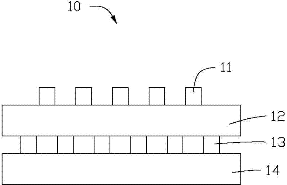
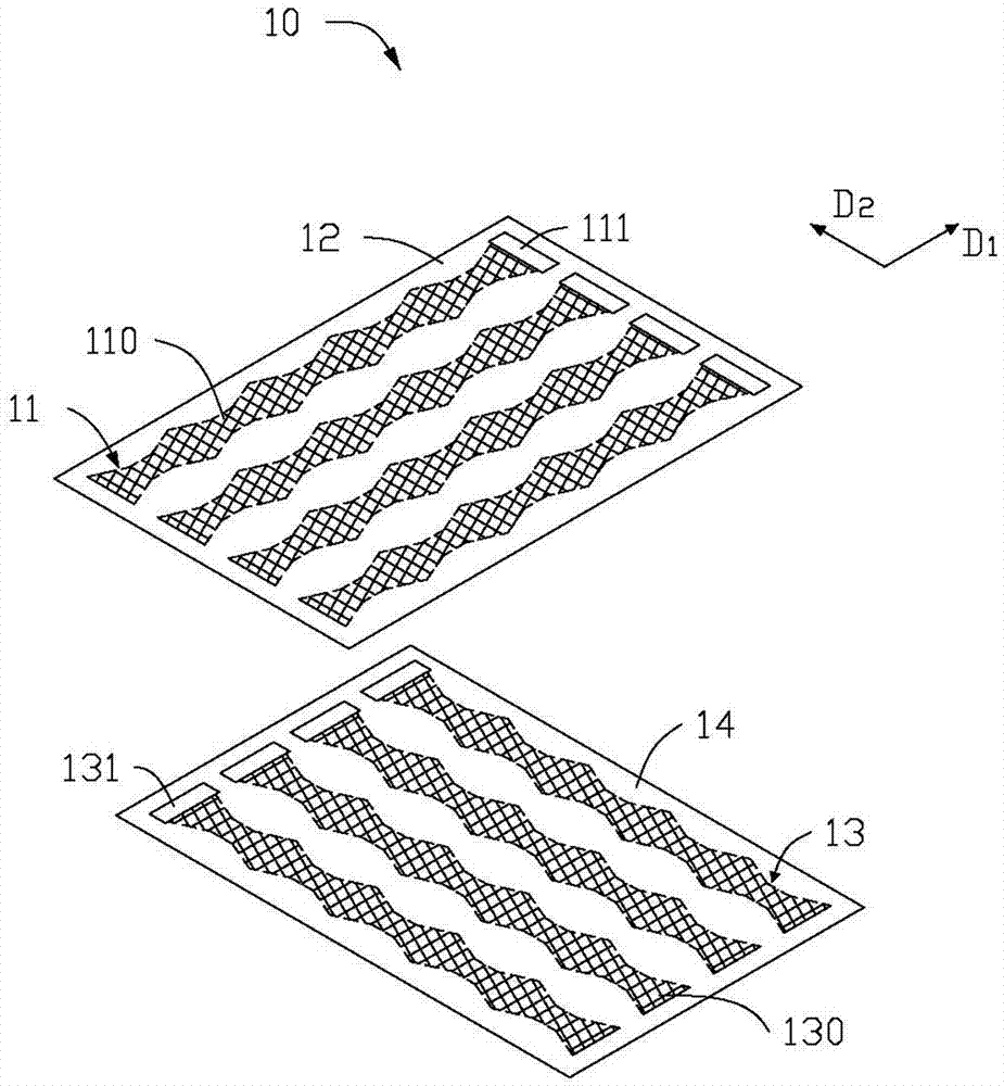
[0023] see figure 1 , is a schematic cross-sectional structure diagram of the touch panel 10 in an embodiment of the present invention. In this embodiment, the touch panel 10 is a capacitive touch panel for detecting user touch operations, starting from the user side The transparent substrate 14 , the second electrode 13 , the transparent insulating substrate 12 and the first electrode 11 are sequentially stacked. The user performs touch operation by touching the transparent substrate 14 . The transparent material used for the transparent insulating substrate 12 and the transparent substrate 14 can be a plastic film or a glass substrate, or other transparent materials. Preferably, the transparent substrate 14 uses a glass substrate, and the transparent insulating substrate 12 can be made of polyethylene terephthalate. (polyethylene terephthalate, PET). It can be understood that the user can add other layer structures according to actual needs, such as disposing a transparent...
PUM
 Abstract
Description
Claims
Application Information
 - R&D
- Intellectual Property
- Life Sciences
- Materials
- Tech Scout
- Unparalleled Data Quality
- Higher Quality Content
- 60% Fewer Hallucinations
Browse by: Latest US Patents, China's latest patents, Technical Efficacy Thesaurus, Application Domain, Technology Topic, Popular Technical Reports.
© 2025 PatSnap. All rights reserved.Legal|Privacy policy|Modern Slavery Act Transparency Statement|Sitemap|About US| Contact US: help@patsnap.com


