Preparing method of amorphous silicon membrane light trapping structure for solar cell
An amorphous silicon thin film, solar cell technology, applied in circuits, photovoltaic power generation, electrical components, etc., can solve the problems of low light absorption efficiency of amorphous silicon solar cells, high reflectivity of amorphous silicon thin films, and increased light absorption, etc. Achieve the effect of easy large-area preparation, mature production process and low cost
- Summary
- Abstract
- Description
- Claims
- Application Information
AI Technical Summary
Problems solved by technology
Method used
Image
Examples
preparation example Construction
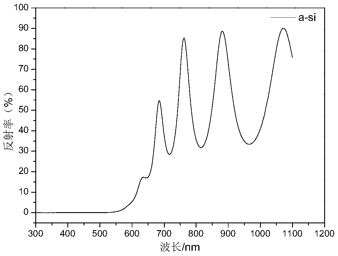
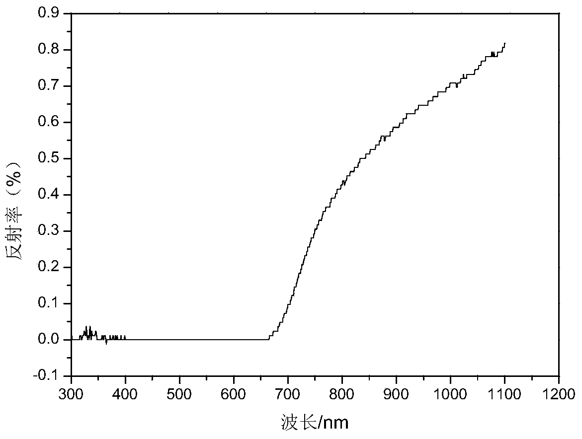
[0020] In order to solve the problem of high reflectivity of the amorphous silicon thin film in the prior art, the present invention provides a new preparation method for the light-trapping structure of the amorphous silicon thin film used in solar cells. Crystalline silicon thin films can form obvious peak structures on the surface of amorphous silicon thin films, which can greatly reduce the reflectivity of amorphous silicon thin films. Broad-spectrum anti-reflection in the entire solar radiation spectral range is achieved, and the suede light-trapping structure prepared by this method has the advantages of easy large-area preparation, mature production technology, and low cost. Specifically, the method for preparing an amorphous silicon thin film light-trapping structure for solar cells includes the following steps:
[0021] A. Cleaning the substrate;
[0022] B. Depositing an amorphous silicon film on the surface of the substrate;
[0023] C. Nanosecond laser scanning is...
Embodiment
[0029] The substrate selected in this embodiment is a glass substrate. The first step is to clean the glass substrate; first, soak the glass substrate in a solution prepared by concentrated sulfuric acid and potassium dichromate to remove heavy metal particles and other impurities; then clean the glass substrate with deionized water; then ultrasonically clean the glass substrate in acetone and absolute ethanol for 15 minutes; finally rinse the substrate repeatedly with deionized water and place it in alcohol for later use, The glass substrate was blown dry with nitrogen.
[0030] In the second step, the PECVD chemical vapor deposition technology is used to deposit an amorphous silicon film on the surface of the substrate; specifically, the glass substrate is first placed in the PECVD reaction chamber and vacuumed to 1*10 -4 Pa, SiH 4 The gas flows into the PECVD reaction chamber at a flow rate of 5 sccm, and the Ar gas flows into the PECVD reaction chamber at a flow rate of 5...
PUM
 Abstract
Description
Claims
Application Information
 - R&D
- Intellectual Property
- Life Sciences
- Materials
- Tech Scout
- Unparalleled Data Quality
- Higher Quality Content
- 60% Fewer Hallucinations
Browse by: Latest US Patents, China's latest patents, Technical Efficacy Thesaurus, Application Domain, Technology Topic, Popular Technical Reports.
© 2025 PatSnap. All rights reserved.Legal|Privacy policy|Modern Slavery Act Transparency Statement|Sitemap|About US| Contact US: help@patsnap.com


