TDI-type CMOS image sensor accumulation circuit for reinforcing single event effect

An image sensor, single-event effect technology, applied in the direction of image communication, television, electrical components, etc., to achieve convenient effects

Inactive Publication Date: 2014-08-13
TIANJIN UNIV
View PDF5 Cites 1 Cited by
  • Summary
  • Abstract
  • Description
  • Claims
  • Application Information

AI Technical Summary

Problems solved by technology

When the TDI type CMOS image sensor is applied in a space environment, the pixel array is also susceptible to the single event effect, but the time-domain redundancy of the TDI accumulation mode itself makes it difficult to shield the interference of a single pixel in the time domain. possible

Method used


Image

  • TDI-type CMOS image sensor accumulation circuit for reinforcing single event effect
  • TDI-type CMOS image sensor accumulation circuit for reinforcing single event effect

Examples


Embodiment Construction

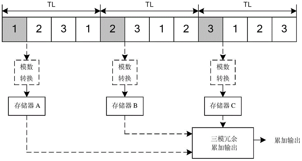
[0012] On the basis of the working sequence of the TDI CMOS image sensor, the present invention proposes a method for strengthening single event effects of pixels based on time domain redundancy. This method requires that the TDI type CMOS image sensor has an integral multiple of 3 accumulation stages. The following describes the simplest three-level accumulation process. Such as figure 2 As shown, for the 3-level accumulation TDI CMOS image sensor, the exposure and readout time of each row is unchanged, but the readout data of the first row and the second row at the interval of TL are firstly converted into digital-to-analog conversion and stored in the memory A And in memory B, after the data read out by the pixels in the third row after TL is quantized and stored in memory C, at this time, memory A, memory B and memory C store three rows of pixels for the same part of the object to be photographed Data output after imaging. The values ​​in the memory A, the memory B and...


PUM


Abstract

The invention relates to the design field of radiation hardened integrated circuits and CMOS image sensors in microelectronics, and provides a working mode of a TDI-type CMOS image sensor, wherein the working mode of the TDI-type CMOS image sensor is used for reinforcing the single event effect of pixels. According to the technical scheme, a TDI-type CMOS image sensor accumulation circuit for reinforcing the single event effect is provided, the accumulative series of the TDI-type CMOS image sensor is 3n, wherein n is equal to 1, 2, 3..., outputs of each line of pixels are stored in corresponding storages after digital-to-analogue conversion is conducted on the outputs, after the 3nth line of pixels is read out, output values of the front n lines of pixels, output values of the middle n lines of pixels and output values of the rear n lines of pixels are accumulated respectively, then three values are accumulated to obtain a sum value, the sum values are sent into a three-mode redundant module to be voted, abnormal values are removed, and the values are accumulated and output; a threshold value used by three-mode redundancy can be set by a user himself / herself. The TDI-type CMOS image sensor accumulation circuit for reinforcing the single event effect is mainly applied to design and manufacturing of integrated circuits.

Description

technical field [0001] The present invention relates to the design field of anti-radiation integrated circuit and CMOS image sensor in microelectronics, especially relates to the anti-radiation reinforcement of TDI image sensor by using circuit design method technical background [0002] The Time-Delay-Integration (TDI) CMOS image sensor uses a linear array or an area array photosensitive array, which moves at a fixed relative speed relative to the object to be photographed, and accumulates the output signals of the pixels of the same part of the object to be photographed. to get the image. figure 1 Shown is the accumulation timing for a 3-stage accumulation, figure 1 The label in represents the row number of each pixel row. In terms of time, each pixel row performs exposure and readout cyclically; TL represents the transit time of the TDI CMOS image sensor, and its value is equal to the center distance between two adjacent rows of pixels divided by The speed at which the ...

Claims


Application Information

Patent Timeline
Patent Type & Authority Applications(China)
IPC IPC(8): H04N5/374H04N5/357
Inventor 姚素英李渊清徐江涛史再峰高静聂凯明高志远
Owner TIANJIN UNIV
Why Eureka
Try Eureka