Array substrate, preparing method thereof and display device

A technology of array substrates and substrate substrates, which is applied in semiconductor/solid-state device manufacturing, electrical components, electric solid-state devices, etc., can solve problems such as poor light transmittance, increase production costs, and reduce production efficiency, so as to reduce the manufacturing process steps, save production costs, and improve production efficiency

Active Publication Date: 2014-07-16
BOE TECH GRP CO LTD +1
View PDF4 Cites 6 Cited by
  • Summary
  • Abstract
  • Description
  • Claims
  • Application Information

AI Technical Summary

Problems solved by technology

In the step of forming the pixel electrode layer, it is generally made of indium tin oxide ITO, indium zinc oxide IZO and other materials, which have good transmittance, but the resistance value is relatively large; while the data line layer is generally made of metals such as molybdenum and aluminum. These metals have the advantage of low resistance, but poor light transmittance
In order to ensure the respective functions of the pixel electrode and the data line, the pixel electrode layer and the data line layer are made of different masks in steps to form the pixel electrode and the data line, and the simultaneous formation of the data line and the pixel electrode cannot be realized.
Therefore, the manufacturing process of the array substrate increases the process steps, increases the production cost, and reduces the production efficiency

Method used


Image

  • Array substrate, preparing method thereof and display device
  • Array substrate, preparing method thereof and display device
  • Array substrate, preparing method thereof and display device

Examples


preparation example Construction

[0044] Such as Figure 4 As shown, the present invention provides a method for preparing an array substrate, comprising the following steps:

[0045] S1. forming a pattern comprising a gate, a gate insulating layer, an active layer, and source and drain electrodes on the base substrate;

[0046] Specifically, in the process of manufacturing the array substrate, the gate electrode, the source electrode, and the drain electrode are made of conductive materials such as metal, and the active layer is made of amorphous silicon (a-Si). The gate insulating layer adopts SiO2, SiN x and other transparent amorphous oxides; the gate, gate insulating layer, active layer, source and drain are respectively produced through a patterning process.

[0047] Further, in step S1, a gate is formed on the base substrate, and a gate line and a gate line connecting line are also formed at the same time.

[0048] S2. Form a transparent conductive layer on the base substrate after step S1, and simul...

Embodiment 1

[0054] This embodiment provides a method for preparing an array substrate, and the specific method is as follows:

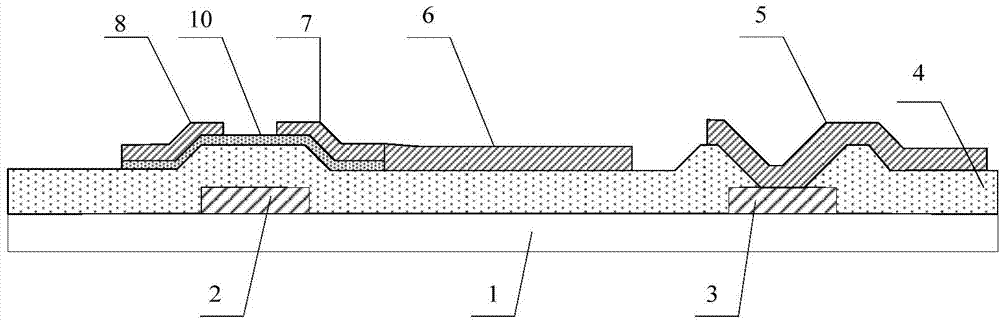
[0055] S1. If figure 1 As shown, a pattern comprising a gate 2, a gate insulating layer 4, an active layer 10, a source 8 and a drain 7 is formed on a base substrate 1;

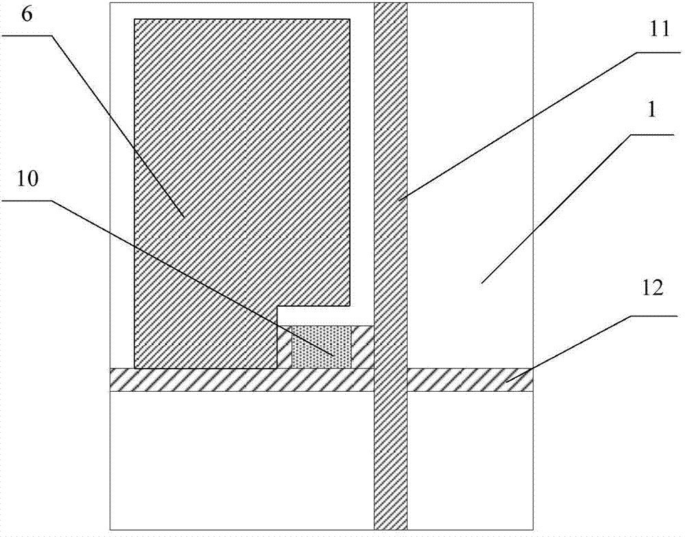
[0056] Further, in step S1, while forming the gate 2, also form such as image 3 grid lines 12 as shown and as figure 1 The grid line connection line 3 shown;

[0057] Specifically, in the process of manufacturing the array substrate, the gate electrode, the source electrode, and the drain electrode are made of conductive materials such as metal, and the active layer is made of amorphous silicon (a-Si). The gate insulating layer adopts SiO2, SiN x and other transparent amorphous oxides; the gate line, the gate line connection line, the gate, the gate insulating layer, the active layer, the source electrode and the drain electrode are respectively manufactured through a patterning process.

...

Embodiment 2

[0073] This embodiment provides a method for preparing an array substrate, including the following steps:

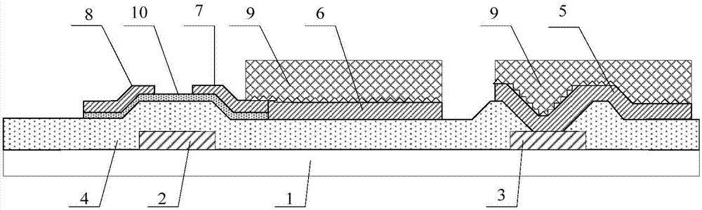
[0074] S1. If figure 1 As shown, a gate 2, a storage capacitor bottom electrode 3, a gate insulating layer 4, an active layer 10, a source 8 and a drain 7 are formed on a substrate 1;

[0075] Further, in step S1, while forming the gate 2, also form such as image 3 grid lines 12 as shown and as figure 1 The grid line connection line 3 shown;

[0076] S2. On the base substrate 1 of step S1, a transparent conductive layer of graphene material is continuously deposited by sputtering; a transparent conductive layer pattern comprising pixel electrodes 6 and data lines 11 is formed simultaneously through a patterning process (or A pattern including the data line, the pixel electrode and the protective layer 5 for protecting the connecting line 3 of the gate line is simultaneously formed through one patterning process).

[0077] Step S2 specifically includes:

[0078] A t...


PUM


Abstract

The invention relates to the technical field of displaying, in particular to an array substrate, a preparing method of the array substrate and a display device. The preparing method of the array substrate comprises the following steps that firstly, a pattern comprising a grid electrode, a grid electrode insulating layer, an active layer, a source electrode and a drain electrode is formed on a substrate body; secondly, a transparent conducting layer is formed on the substrate body on which the first step is carried out, and a pattern comprising a pixel electrode and a data line is formed through the one-time pattern composition technology. According to the array substrate, the pixel electrode and the data line are formed through the one-time pattern composition technology at the same time, the steps of the manufacturing technology are reduced, production cost is reduced, and production efficiency is improved; furthermore, the transparent conducting layer is made of graphene or nanometer silver wire materials, and the pixel electrode and the data line are formed, so that the pixel electrode and the data line have low resistance values and high light transmissivity, and the performance of the array substrate is improved.

Description

technical field [0001] The present invention relates to the field of display technology, in particular to an array substrate, a preparation method thereof, and a display device. Background technique [0002] In the manufacturing process of the thin film transistor-liquid crystal display array substrate, it includes forming gates and gate lines, gate insulating layers, gate insulating layer via holes, active layers, source and drain electrode layers and data lines on the substrate substrate, and pixel electrodes. In the step of forming the pixel electrode layer, it is generally made of indium tin oxide ITO, indium zinc oxide IZO and other materials, which have good transmittance, but the resistance value is too large; and the data line layer is generally made of metals such as molybdenum and aluminum. These metals have the advantage of low resistance, but poor light transmission. In order to ensure the respective functions of the pixel electrode and the data line, the pixel...

Claims


Application Information

Patent Timeline
Patent Type & Authority Applications(China)
IPC IPC(8): H01L21/77H01L27/12
CPCH01L27/1288H01L27/124H01L27/1259
Inventor 郭建
Owner BOE TECH GRP CO LTD
Why Eureka
Try Eureka