Method for measuring activation energy of resistive random access memory
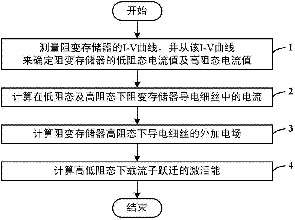
A technology of resistive memory and activation energy, applied in static memory, instruments, etc., can solve the problems of activation energy error, inability to distinguish activation energy, inability to analyze carrier transport characteristics in resistive memory, etc., to reduce The effect of measurement error
- Summary
- Abstract
- Description
- Claims
- Application Information
AI Technical Summary
Problems solved by technology
Method used
Image
Examples
Embodiment 1
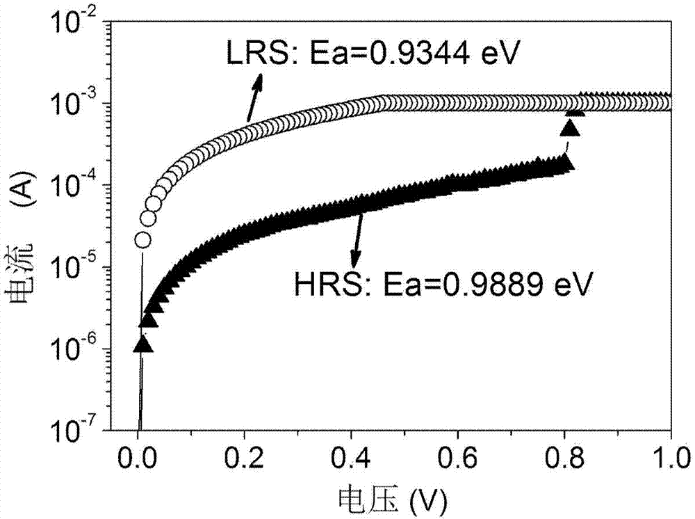
[0065] With W / Ti / HfO 2 / Pt device as an example, first obtain the I-V characteristics under the state of HRS and LRS by electrical method measurement, then pass the read voltage of 0.1V, obtain the current value under the low resistance state when the read voltage is 1.97×10 -4 A, the current value in the high resistance state is 1.14×10 -5 A, will be 1.97×10 -4 Calculation is performed in formula (1) of A generation, and the activation energy of the carrier transition in the low-resistance state is obtained; the 1.14×10 -5 A is substituted into formulas (3) and (4), and then combined with formulas (2)-(5) to calculate the activation energy of the carrier transition in the high-impedance state. The result is as figure 2 As shown, in the low-resistance state (LRS), the activation energy of carrier transition is Ea=0.9344eV, and in the high-resistance state (HRS), the activation energy of carrier transition is Ea=0.9889eV. The parameters used in the calculation are: the tem...
Embodiment 2
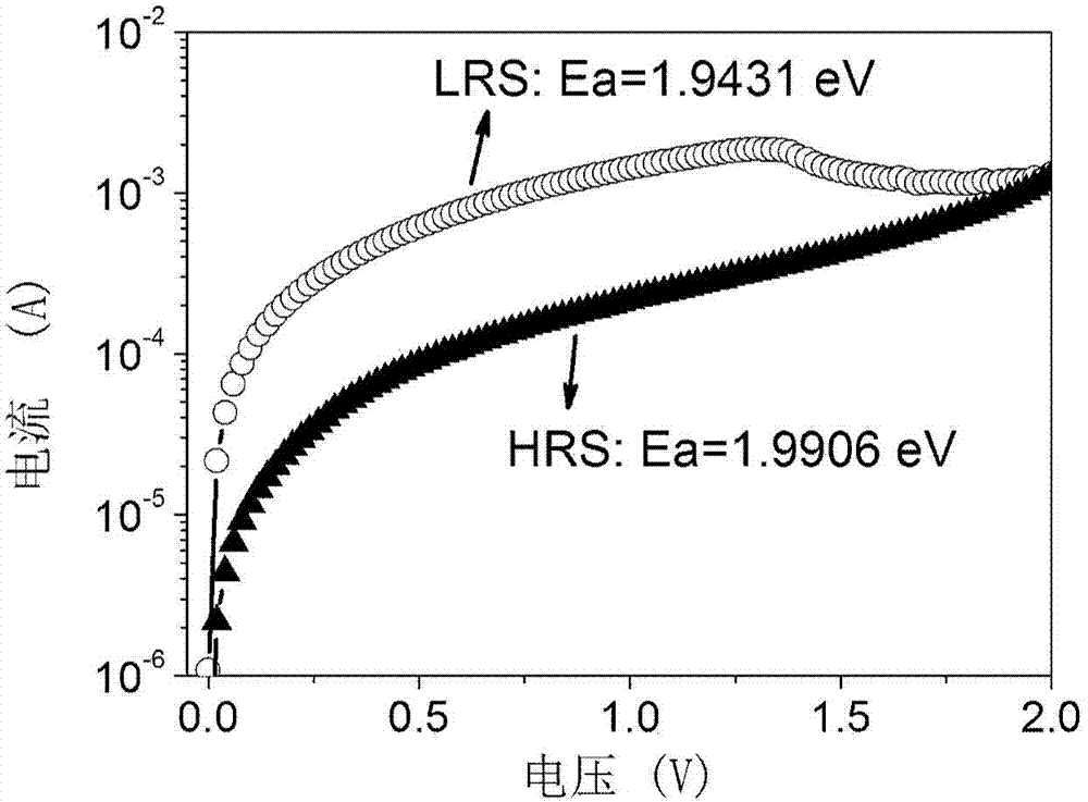
[0067] With TiN / ZrO 2 / Pt device as an embodiment, then through the reading voltage of 0.1V, the current value in the low resistance state when obtaining the reading voltage is 1.09×10 -4 A, the current value in the high resistance state is 1.17×10 -5 A; will be 1.09×10 -4 Calculation is carried out in the formula (1) of A generation, and the activation energy of the carrier transition in the low-resistance state is obtained; the 1.17×10 -5 A is substituted into formulas (3) and (4), and then combined with formulas (2)-(5) to calculate the activation energy of the carrier transition in the high-impedance state. The result is as image 3 As shown, in the low resistance state (LRS), the activation energy of the carrier transition is Ea=1.9431eV, and in the high resistance state (HRS), the activation energy of the carrier transition is Ea=1.9906eV. The parameters used in the calculation are: the temperature is T=300K, V=0.1V, σ 0 =10 13 S / m, α -1 = 1.5nm, R ij = 0.385nm, ...
Embodiment 3
[0069] Cu / WO 3 / Pt device as an embodiment, then through the reading voltage of 0.1V, the current value in the low resistance state when obtaining the reading voltage is 2.0×10 -7 A, the current value in the high resistance state is 2.04×10 -8 A; put 2.0×10 -7 Calculation is performed in formula (1) of A generation to obtain the activation energy of the carrier transition in the low-resistance state; the 2.04×10 -8 A is substituted into formulas (3) and (4), and then combined with formulas (2)-(5) to calculate the activation energy of the carrier transition in the high-impedance state. The result is as Figure 4 As shown, in the low resistance state (LRS), the activation energy of carrier transition is Ea=0.7352eV, and in the high resistance state (HRS), the activation energy of carrier transition is Ea=0.7953eV. The parameters used in the calculation are: the temperature is T=300K, V=0.1V, σ 0 =10 13 S / m, α -1 = 1.5nm, R ij = 0.385nm, ε = 35, μ 0 =150m 2 / Vs, L=50nm...
PUM
| Property | Measurement | Unit |
|---|---|---|
| Thickness | aaaaa | aaaaa |
| Thickness | aaaaa | aaaaa |
| Thickness | aaaaa | aaaaa |
Abstract
Description
Claims
Application Information
 - R&D Engineer
- R&D Manager
- IP Professional
- Industry Leading Data Capabilities
- Powerful AI technology
- Patent DNA Extraction
Browse by: Latest US Patents, China's latest patents, Technical Efficacy Thesaurus, Application Domain, Technology Topic, Popular Technical Reports.
© 2024 PatSnap. All rights reserved.Legal|Privacy policy|Modern Slavery Act Transparency Statement|Sitemap|About US| Contact US: help@patsnap.com


