
Structure with realization of 3D interlayer vertical interconnection by using flexible substrate and manufacturing method thereof

A technology that uses flexible and vertical interconnection, applied in semiconductor/solid-state device manufacturing, semiconductor/solid-state device components, semiconductor devices, etc., can solve problems such as increased BGA crosstalk, increased return loss, and restrictions on high-frequency signal transmission , to achieve the effect of improving shielding performance, reducing attenuation amplitude and increasing transmission rate

Inactive Publication Date: 2014-06-25
INST OF MICROELECTRONICS CHINESE ACAD OF SCI +1
View PDF3 Cites 3 Cited by
  • Summary
  • Abstract
  • Description
  • Claims
  • Application Information

AI Technical Summary

Problems solved by technology

The larger the BGA is, the more serious the discontinuity is, and the transmission loss increases at high frequencies, and the return loss also increases, which restricts the transmission of high-frequency signals, especially the transmission of radio frequency signals.
With the decrease of BGA spacing, on the one hand, the risk of soldering increases, causing short circuits, and on the other hand, the crosstalk between BGAs also increases, affecting signal integrity
The spacing between BGA solder balls is standard, and according to different application standards, the property definitions of BGA solder balls are fixed, so it is difficult to use BGA to shield signals in three-dimensional packages.
Therefore, the shielding of the chip by the BGA is generally combined with an open cavity. Refer to the US patent US20020096767. Such an open cavity is better than a simple BGA shielding effect, but due to the existence of the BGA, it is possible to couple a certain amount of electromagnetic waves from the BGA, so the BGA The problems of signal discontinuity, signal crosstalk and signal attenuation are still difficult to solve

Method used


Image

  • Structure with realization of 3D interlayer vertical interconnection by using flexible substrate and manufacturing method thereof
  • Structure with realization of 3D interlayer vertical interconnection by using flexible substrate and manufacturing method thereof

Examples


Embodiment 1

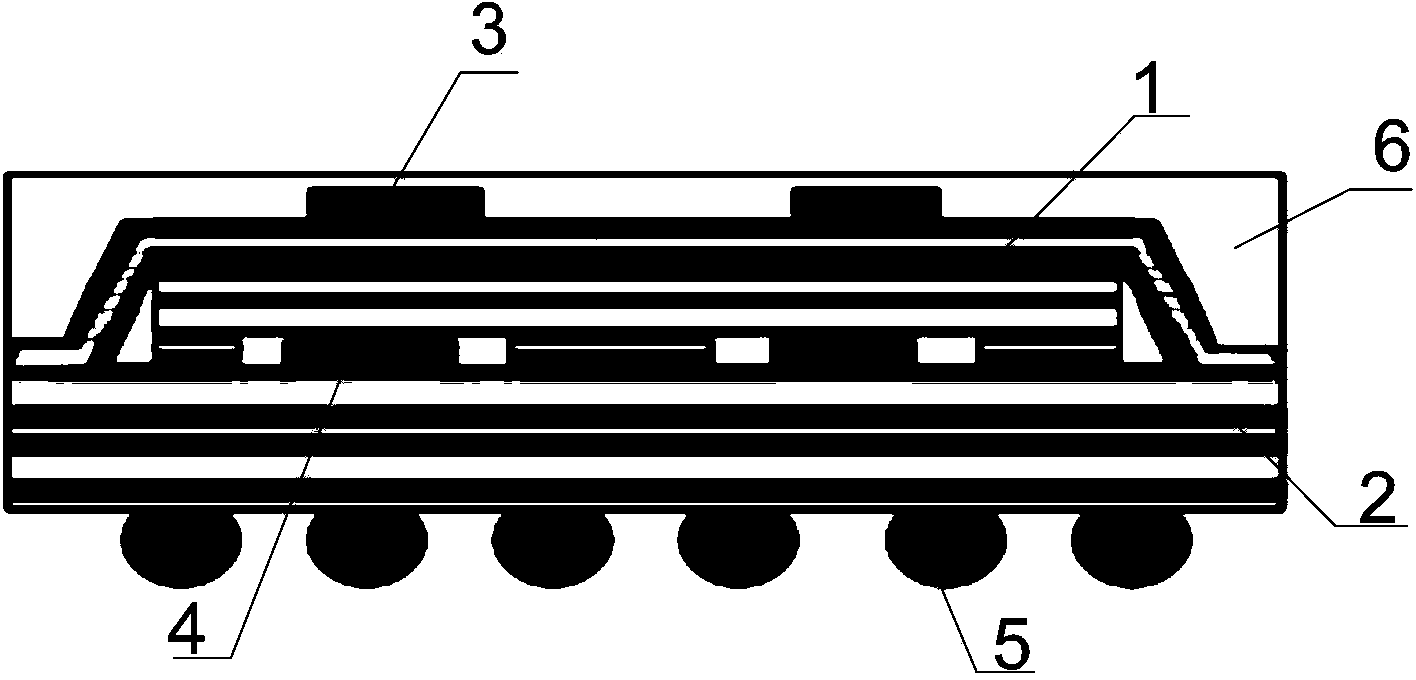
[0016] see figure 1 , this embodiment provides a structure using a flexible substrate to realize vertical interconnection between three-dimensional layers, including a first printed circuit board 1, a second printed circuit board 2, a first device 3 (such as a radio frequency component), a second Two devices 4 (such as radio frequency components), solder balls 5 and plastic sealing layer 6 . The first printed circuit board 1 is a flexible printed circuit board or a rigid-flexible printed circuit board, wherein the flexible part of the rigid-flexible printed circuit board is arranged at the upper, lower or middle position of the rigid part (this In the embodiment, a rigid-flex printed circuit board is selected, and the flexible part is arranged directly above the rigid part, and the length of the flexible part is greater than the length of the rigid part). The rigid part of the rigid-flexible printed circuit board has a certain thickness, which allows subsequent opening of gro...

Embodiment 2

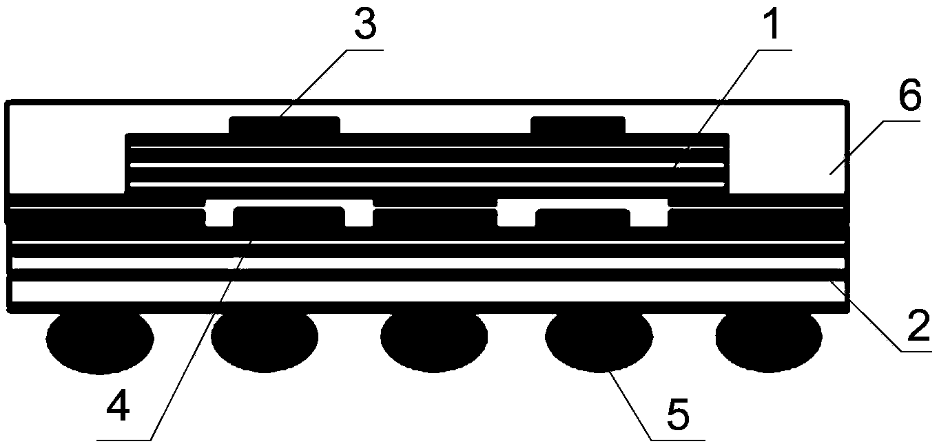
[0025] see figure 2, this embodiment provides a structure using a flexible substrate to realize vertical interconnection between three-dimensional layers, including a first printed circuit board 1, a second printed circuit board 2, a first device 3 (such as a radio frequency component), a second Two devices 4 (such as radio frequency components), solder balls 5 and plastic sealing layer 6 . The first printed circuit board 1 is a flexible printed circuit board or a rigid-flexible printed circuit board, wherein the flexible part of the rigid-flexible printed circuit board is arranged at the upper, lower or middle position of the rigid part (this In the embodiment, a rigid-flex printed circuit board is selected, and the flexible part is arranged directly below the rigid part, and the length of the flexible part is equal to the length of the rigid part). The rigid part of the rigid-flexible printed circuit board has a certain thickness, which allows subsequent opening of grooves...


PUM


Abstract

The invention relates to the technical field of electronic packaging and particularly relates to a structure with the realization of 3D interlayer vertical interconnection by using a flexible substrate and a manufacturing method thereof. The structure comprises a first printed circuit board, a second printed circuit board, a first device, a second device, a soldered ball and a lamination structure. The second device is installed above the second printed circuit board. The first printed circuit board is fixed above the second printed circuit board, and the second device is arranged in a groove. The first device is fixed above the first printed circuit board. The lamination layer covers the first printed circuit board, the second printed circuit board and the outer side of the first device. The soldered ball is arranged at the bottom of the second printed circuit board. The invention provides the structure with the realization of 3D interlayer vertical interconnection by using the flexible substrate and the manufacturing method, the discontinuity and impedance mismatching of signals can be reduced, thus the transmission rate of the signals is greatly improved, higher bandwidth is supported, and the interconnection density of the flexible substrate is higher.

Description

technical field [0001] The invention relates to the technical field of electronic packaging, in particular to a structure and a manufacturing method for realizing vertical interconnection between three-dimensional layers by using a flexible substrate. Background technique [0002] BGA (Ball Grid Array, printed circuit board with ball grid array structure) is an impedance discontinuity point on the signal interconnection. The size and shape of BGA affect the signal integrity of high-frequency transmission. The larger the BGA is, the more serious the discontinuity is, and the transmission loss increases at high frequencies, and the return loss also increases, which restricts the transmission of high-frequency signals, especially the transmission of radio frequency signals. With the decrease of BGA spacing, on the one hand, the risk of soldering is increased, causing short circuit, and on the other hand, the crosstalk between BGAs also increases, which affects signal integrity....

Claims


Application Information

Patent Timeline
IPC IPC(8): H01L23/498H01L23/552H01L21/50H01L21/60
CPCH01L2924/15311H01L2224/16225
Inventor 刘丰满曹立强
Owner INST OF MICROELECTRONICS CHINESE ACAD OF SCI
Learn More