Crystal silicon cell double-layer passivation anti-reflection structure
A crystalline silicon battery and double-layer film technology, which is applied in the direction of circuits, photovoltaic power generation, electrical components, etc., can solve the problems of large incident light loss, single-layer film anti-reflection effect and passivation effect are not very ideal, so as to reduce reflection Effect
- Summary
- Abstract
- Description
- Claims
- Application Information
AI Technical Summary
Problems solved by technology
Method used
Image
Examples
Embodiment Construction
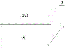
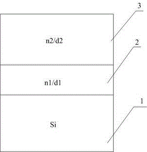
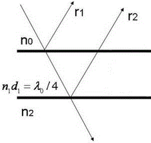
[0014] Accompanying drawing is a kind of specific embodiment of the present invention. The double-layer passivation antireflection structure of the crystalline silicon cell is characterized in that: the surface of the crystalline silicon cell 1 is coated with two layers of silicon nitride films, the lower layer of silicon nitride film 2 and the lower layer of silicon nitride film above the crystalline silicon cell 1 2 above the upper silicon nitride film 3, the thickness of the lower silicon nitride film 3 is d 2 , the refractive index n 2 , the thickness d of the upper silicon nitride film 3 1 , the refractive index n 1 , and d 1 >d 2 , n 1 2 ; the n 1 , n 2 、d 2 The relationship is n 1 2 =n 0 no 2 , where n 0 is the refractive index of air, n 1 d 1 =λ 0 / 4, λ 0 is the wavelength of the incident light. Because the refractive index of the lower silicon nitride film 2 is large, and its own extinction coefficient is large, it will absorb part of the short wave,...
PUM
 Abstract
Description
Claims
Application Information
 - R&D
- Intellectual Property
- Life Sciences
- Materials
- Tech Scout
- Unparalleled Data Quality
- Higher Quality Content
- 60% Fewer Hallucinations
Browse by: Latest US Patents, China's latest patents, Technical Efficacy Thesaurus, Application Domain, Technology Topic, Popular Technical Reports.
© 2025 PatSnap. All rights reserved.Legal|Privacy policy|Modern Slavery Act Transparency Statement|Sitemap|About US| Contact US: help@patsnap.com


