Output buffering circuit, array substrate and display device
一种输出缓冲、电路的技术,应用在放大装置的零部件、电气元件、静态指示器等方向,能够解决没有反馈电路、稳定性差、功耗大等问题
- Summary
- Abstract
- Description
- Claims
- Application Information
AI Technical Summary
Problems solved by technology
Method used
Image
Examples
Embodiment Construction
[0035] The specific implementation manners of the present invention will be further described in detail below in conjunction with the accompanying drawings and embodiments. The following examples are used to illustrate the present invention, but are not intended to limit the scope of the present invention.
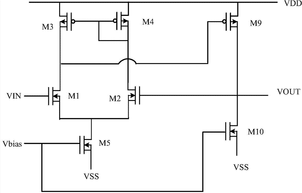
[0036] At present, the normal output voltage of the output buffer circuit of the driving voltage VOFF of the TFT-LCD gate driver is -8V, and an external voltage stabilizing capacitor is required. Such as figure 1 As shown, the first-stage operational amplifier circuit is a differential input circuit composed of five transistors M1~M5, and the second-stage operational amplifier circuit uses a common-source amplifier circuit with an active load composed of two transistors M9 and M10. For higher gain and larger output voltage swing. In order to reduce the static power consumption and the bias current of M10 and M9 is small, the voltage negative feedback forms a unity-gain a...
PUM
 Abstract
Description
Claims
Application Information
 - R&D
- Intellectual Property
- Life Sciences
- Materials
- Tech Scout
- Unparalleled Data Quality
- Higher Quality Content
- 60% Fewer Hallucinations
Browse by: Latest US Patents, China's latest patents, Technical Efficacy Thesaurus, Application Domain, Technology Topic, Popular Technical Reports.
© 2025 PatSnap. All rights reserved.Legal|Privacy policy|Modern Slavery Act Transparency Statement|Sitemap|About US| Contact US: help@patsnap.com


