Plasma treatment method

A technology of plasma and processing method, which is applied in the field of microelectronics, can solve the problems of increasing the roughness of the side wall of the substrate, adverse effects of the process, uneven line width of the groove or hole, etc., and achieve the effect of reducing the roughness of the side wall

Inactive Publication Date: 2014-05-14
BEIJING NAURA MICROELECTRONICS EQUIP CO LTD
View PDF5 Cites 0 Cited by
  • Summary
  • Abstract
  • Description
  • Claims
  • Application Information

AI Technical Summary

Problems solved by technology

The formed fan-shaped morphology will cause uneven line width of the groove or hole, which in turn will have a negative impact on the subsequent process
[0004] To sum up, in the prior art, after the deep silicon etching process, fan-shaped topography is formed on the side wall of the substrate, thereby increasing the roughness of the side wall of the substrate.

Method used


Image

  • Plasma treatment method
  • Plasma treatment method
  • Plasma treatment method

Examples


Embodiment Construction

[0025] In order to enable those skilled in the art to better understand the technical solution of the present invention, the plasma treatment method provided by the present invention will be described in detail below with reference to the accompanying drawings.

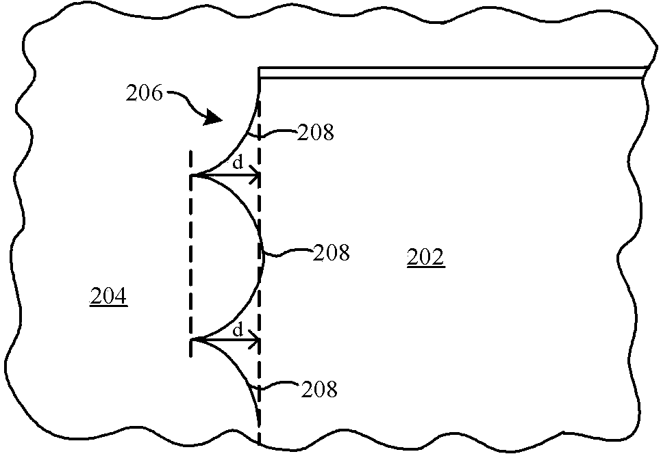
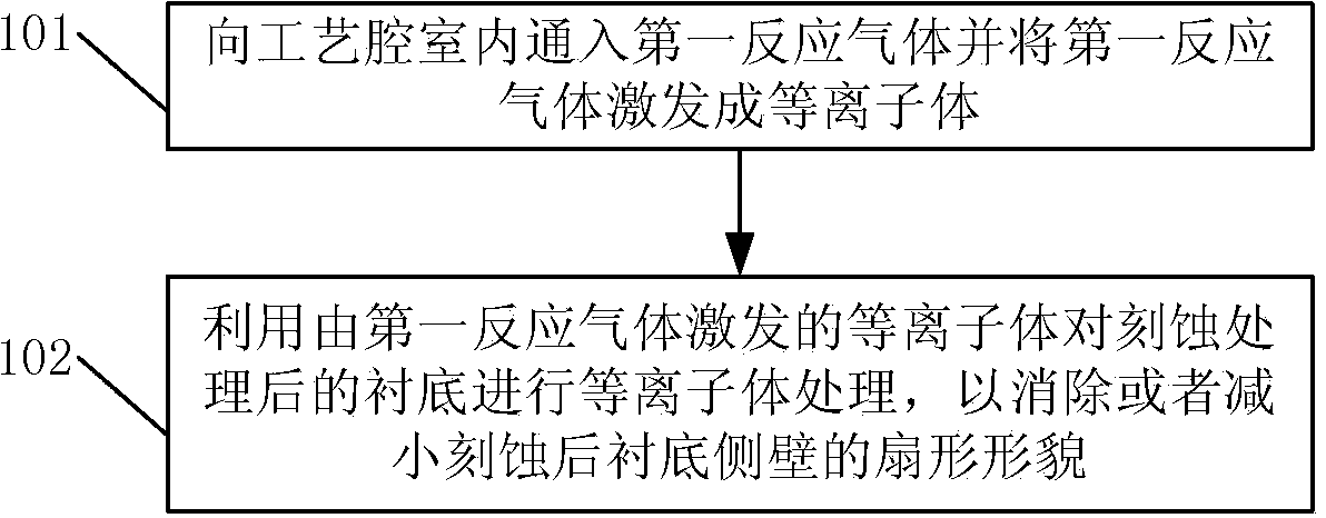
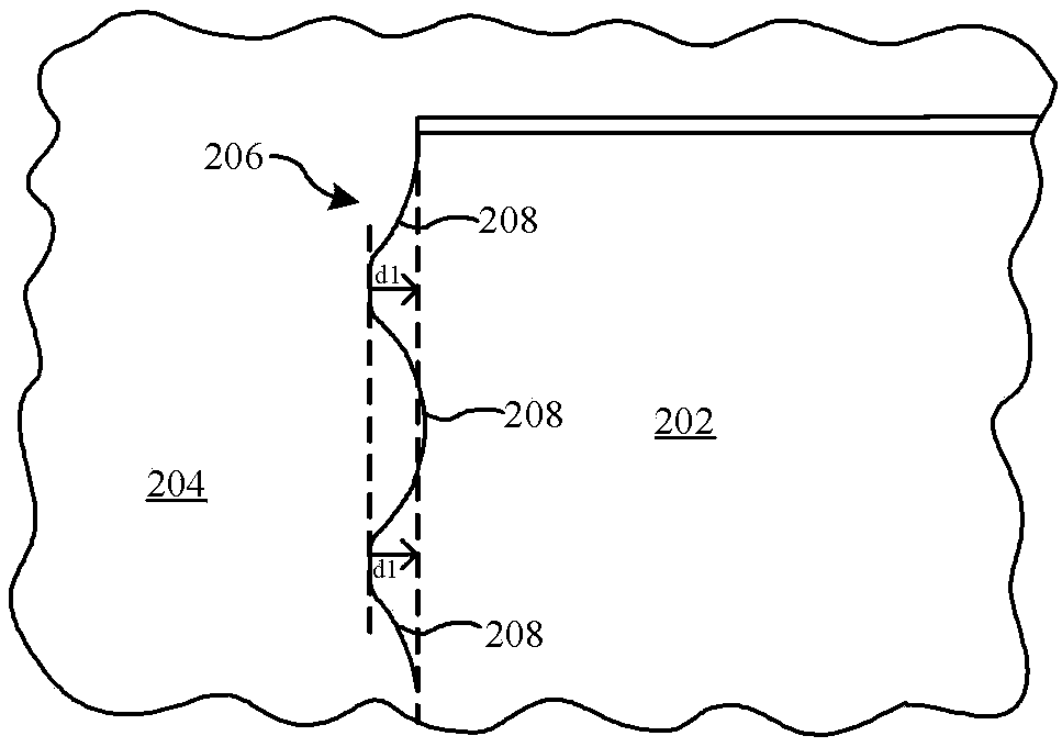
[0026] figure 2 A flow chart of a plasma treatment method provided in Embodiment 1 of the present invention, such as figure 2 As shown, the method includes:

[0027] Step 101 , injecting a first reaction gas into the process chamber and exciting the first reaction gas into plasma.

[0028] The method provided in this embodiment can be implemented by a plasma processing device. The plasma processing equipment may include a process chamber, an upper radio frequency power supply for supplying power of the upper radio frequency power supply to the process chamber, and a gas introduction device for introducing reaction gas into the process chamber. Further, the plasma processing equipment further includes a lower radi...


PUM


Abstract

The invention discloses a plasma treatment method. The plasma treatment method comprises the following steps: introducing a first reaction gas into a process chamber; and carrying out plasma treatment of a substrate etched by the first reaction gas in order to remove the sector morphology. In the technical scheme of the plasma treatment method provided by the invention, the substrate etched by the first reaction gas is subjected to the plasma treatment in order to eliminate or reduce the sector morphology, so the roughness of the sidewall of the substrate is greatly reduced.

Description

technical field [0001] The invention relates to the technical field of microelectronics, in particular to a plasma treatment method. Background technique [0002] With Micro-Electro-Mechanical Systems (hereinafter referred to as: MEMS) being more and more widely used in automotive and consumer electronics fields and TSV through-hole etching (ThroughSilicon Etch) technology has more and more prospects in the future packaging field The more extensive, the dry plasma silicon deep etching process has gradually become one of the hottest processes in the field of MEMS processing and TSV technology. The main difference between the silicon deep etching process and the general silicon etching process is that the etching depth of the silicon deep etching process is much larger than that of the general etching process, and the etching depth of the silicon deep etching process is generally tens of microns or even up to Hundreds of microns, while the etching depth of the general silicon...

Claims


Application Information

Patent Timeline
Patent Type & Authority Applications(China)
IPC IPC(8): C23F4/00B81C1/00H01L21/3065
Inventor 蒋中伟
Owner BEIJING NAURA MICROELECTRONICS EQUIP CO LTD
Why Eureka
Try Eureka