Multi-state Gallium Antimony-Stin Selenide Multilayer Nanocomposite Phase Change Material and Its Preparation and Application
A nano-composite, phase-change material technology, applied in the field of microelectronic materials, can solve the problem that the power consumption of phase-change memory devices is not too large, and achieve improved thermal stability, high crystalline and amorphous resistance, The effect of increasing storage density
- Summary
- Abstract
- Description
- Claims
- Application Information
AI Technical Summary
Problems solved by technology
Method used
Image

Examples
Embodiment 1
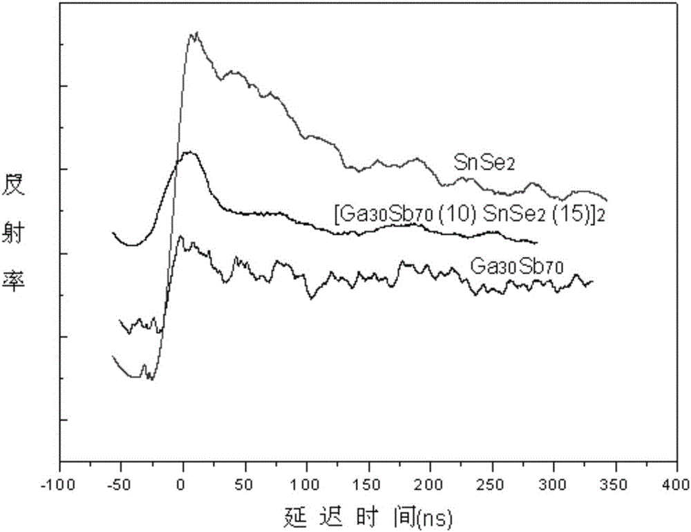
[0049] Ga prepared in this example 30 Sb 70 / SnSe 2 The total thickness of the nanocomposite multilayer phase change film is 50nm, and the specific structure is [Ga 30 Sb 70 (10nm)SnSe 2 (15nm)] 2.
[0050] 1. Clean SiO2 2 / Si(100) substrate surface and back, remove dust particles, organic and inorganic impurities:
[0051] (a) Place the substrate in an ethanol solution, and clean it ultrasonically for 15 minutes to remove dust particles and inorganic impurities on the surface of the substrate;
[0052] (b) The substrate is placed in an acetone solution, and ultrasonically cleaned for 15 minutes to remove organic impurities on the surface of the substrate;
[0053] (c) Place the substrate in deionized water, clean it ultrasonically for 15 minutes, and clean the surface again;
[0054] (d) Take out the substrate, dry it with pure Ar gas, and set it aside.
[0055] 2. Prepared by sputtering method [Ga 30 Sb 70 (10nm)SnSe 2 (15nm)] 2 film preparation
[0056] (a) put...
Embodiment 2
[0065] Ga prepared in this example30 Sb 70 / SnSe 2 The total thickness of the nanocomposite multilayer phase change film is 50nm, and the specific structure is [Ga 30 Sb 70 (25nm)SnSe 2 (25nm)]1.
[0066] 1. Clean SiO2 2 / Si(100) substrate surface and back, remove dust particles, organic and inorganic impurities:
[0067] (a) Place the substrate in an ethanol solution, and clean it ultrasonically for 15 minutes to remove dust particles and inorganic impurities on the surface of the substrate;
[0068] (b) The substrate is placed in an acetone solution, and ultrasonically cleaned for 15 minutes to remove organic impurities on the surface of the substrate;
[0069] (c) Place the substrate in deionized water, clean it ultrasonically for 15 minutes, and clean the surface again;
[0070] (d) Take out the substrate, dry it with pure Ar gas, and set it aside.
[0071] 2. Prepared by sputtering method [Ga 30 Sb 70 (25nm)SnSe 2 (25nm)] 1 film preparation
[0072] (a) put Ga...
Embodiment 3
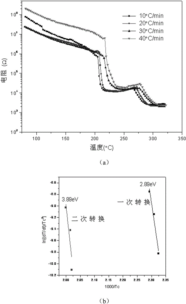
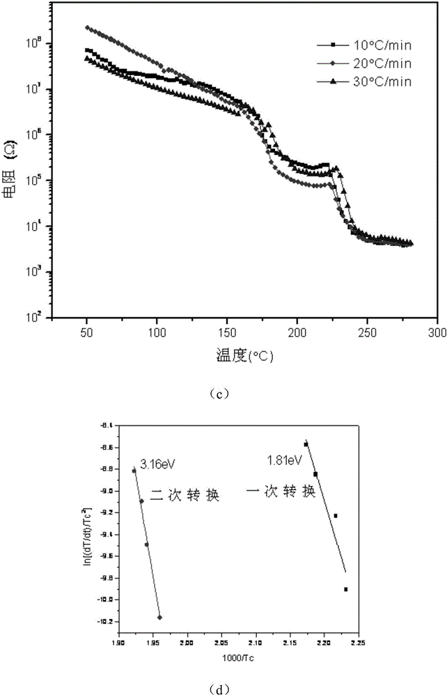
[0111] Polymorphic gallium antimony-tin selenide multilayer nanocomposite phase change material, Ga 30 Sb 70 / SnSe 2 Nanocomposite multilayer phase change films made of SnSe 2 thin film and Ga 30 Sb 70 The films are alternately arranged into a multilayer film structure, in which the SnSe 2 The thickness of the film is 5nm, Ga 30 Sb 70 The thickness of the film is 5nm; it consists of 5 layers of periodically repeating structure, Ga 30 Sb 70 / SnSe 2 The total thickness of the nanocomposite multilayer phase change film is 50nm, Ga 30 Sb 70 / SnSe 2 The nanocomposite multilayer phase change film has three storage states.
[0112] The multi-state gallium antimony-tin selenide multilayer nanocomposite phase change material was prepared by magnetron sputtering method. 2 / Si(100) substrate, with Ga 30 Sb 70 and SnSe 2 As the sputtering target, Ar gas was used as the sputtering gas to alternately deposit multiple layers of SnSe 2 thin film and Ga 30 Sb 70 Thin film, d...
PUM
| Property | Measurement | Unit |
|---|---|---|
| Thickness | aaaaa | aaaaa |
| Thickness | aaaaa | aaaaa |
| Total thickness | aaaaa | aaaaa |
Abstract
Description
Claims
Application Information
 - R&D
- Intellectual Property
- Life Sciences
- Materials
- Tech Scout
- Unparalleled Data Quality
- Higher Quality Content
- 60% Fewer Hallucinations
Browse by: Latest US Patents, China's latest patents, Technical Efficacy Thesaurus, Application Domain, Technology Topic, Popular Technical Reports.
© 2025 PatSnap. All rights reserved.Legal|Privacy policy|Modern Slavery Act Transparency Statement|Sitemap|About US| Contact US: help@patsnap.com