Lateral Power Devices with Composite Gate Dielectrics

A technology of lateral power devices and compound gate dielectrics, applied in semiconductor devices, electrical components, circuits, etc., can solve problems such as hindering performance improvement, power consumption increase, energy density increase, etc., to reduce on-state resistance, increase channel channel current, and the effect of improving the cross-over characteristics

Active Publication Date: 2016-08-17
SHANGHAI SIMGUI TECH
View PDF3 Cites 0 Cited by
  • Summary
  • Abstract
  • Description
  • Claims
  • Application Information

AI Technical Summary

Problems solved by technology

[0004] In the 65nm era, leakage has always been an important factor that reduces the yield rate of processors, hinders performance improvement and reduces power consumption
As the processor adopts a 45nm process, the corresponding core area will decrease, resulting in a substantial increase in the energy density per unit area, and the leakage problem will become more prominent. If it is not solved well, the power consumption will increase accordingly.
However, the traditional silicon dioxide gate dielectric process can no longer meet the requirements of 45nm processors. Therefore, in order to solve the leakage problem well, at present, on the 28nm process node, a high dielectric constant metal gate (HKMG) structure is used to replace Traditional silicon dioxide gate dielectric and polysilicon structure have been recognized as the main and only means to solve the problems of gate leakage current, polysilicon loss and boron penetration
However, the high dielectric constant metal gate (HKMG) structure is slightly insufficient in improving the channel carrier mobility. It is necessary to optimize the device structure to reduce the on-state resistance and improve the transconductance characteristics of the device.

Method used


Image

  • Lateral Power Devices with Composite Gate Dielectrics

Examples


Embodiment Construction

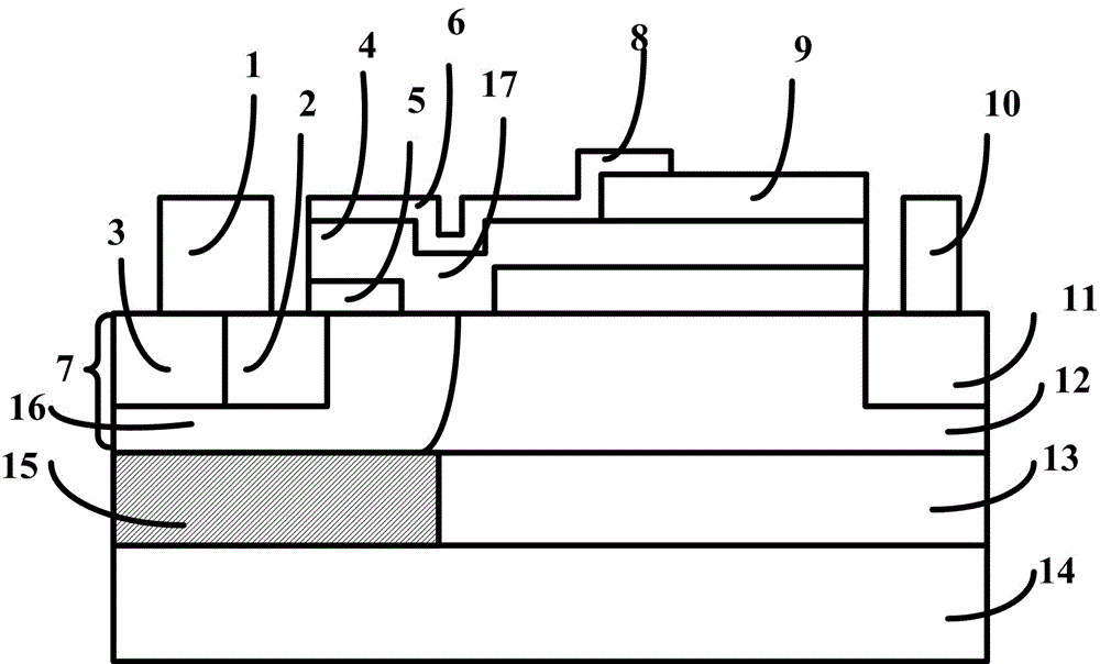
[0016] The specific implementation manner of the lateral power device with composite gate dielectric provided by the present invention will be described in detail below with reference to the accompanying drawings.

[0017] Reference attached figure 1 is a schematic diagram of a lateral power device with a composite gate dielectric according to this specific embodiment. Comprising a semiconductor substrate 14, an insulating buried layer 13 located on the surface of the semiconductor substrate 14, an active layer 7 located on the surface of the insulating buried layer 13, a gate dielectric layer located on the surface of the active layer 7, and located on the The gate electrode 6 on the surface of the gate dielectric layer and the source electrode 1 and the drain electrode 10 positioned on both sides of the gate electrode 6, the gate dielectric layer includes a high dielectric constant dielectric 4 and SiO on one side of the source electrode 1 2 A composite first gate dielectri...


PUM


Abstract

A transverse power device with composite grid media comprises a semiconductor substrate, an insulation burying layer on the surface of the semiconductor substrate, an active layer on the surface of the insulation burying layer, a grid medium layer on the surface of the active layer, a grid electrode on the surface of the grid medium layer, a source electrode and a drain electrode, the source electrode and the drain electrode are arranged on the two sides of the grid electrode, the grid medium layer comprises a first grid medium on one side of the source electrode and a second grid medium arranged on one side of the drain electrode, and the equivalent grid oxygen thickness of the first grid medium is larger than that of the second grid medium. The first grid medium makes contact with the second grid medium. The device has the advantages that the composite grid medium structure can reduce ON resistance, and the transconductances of the device are improved. .

Description

technical field [0001] The invention relates to a lateral power device with a composite gate dielectric, belonging to the technical field of microelectronics and solid electronics. Background technique [0002] Power integrated circuits are sometimes called high-voltage integrated circuits, which are an important branch of modern electronics. They can provide new circuits with high speed, high integration, low power consumption and radiation resistance for various power conversion and energy processing devices, and are widely used in electric power Daily consumption fields such as control systems, automotive electronics, display device drivers, communications and lighting, as well as many important fields such as national defense and aerospace. The rapid expansion of its application scope has also put forward higher requirements for the high-voltage devices in its core part. In power integrated circuits, lateral double-diffused metal-oxide-semiconductor field-effect transis...

Claims


Application Information

Patent Timeline
Patent Type & Authority Patents(China)
IPC IPC(8): H01L29/423H01L29/51
CPCH01L29/42356H01L29/42364
Inventor 魏星徐大伟狄增峰方子韦
Owner SHANGHAI SIMGUI TECH
Why Eureka
Try Eureka