Transistor Accelerated Life Test and Operating Point Stability System

An accelerated life test, transistor technology, used in control/regulation systems, single semiconductor device testing, non-electric variable control, etc., can solve problems such as low efficiency, high cost, and long test cycle, and achieve the effect of avoiding damage

Inactive Publication Date: 2016-06-01
BEIJING UNIV OF TECH
View PDF5 Cites 0 Cited by
  • Summary
  • Abstract
  • Description
  • Claims
  • Application Information

AI Technical Summary

Problems solved by technology

However, the current life test (such as identification test and acceptance test, etc.) has a long test period, high cost and low efficiency.

Method used


Image

  • Transistor Accelerated Life Test and Operating Point Stability System
  • Transistor Accelerated Life Test and Operating Point Stability System
  • Transistor Accelerated Life Test and Operating Point Stability System

Examples


Embodiment Construction

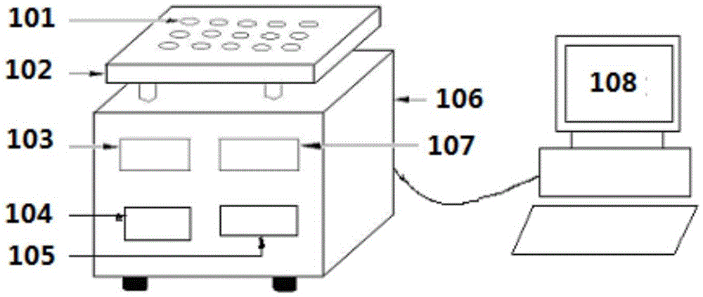
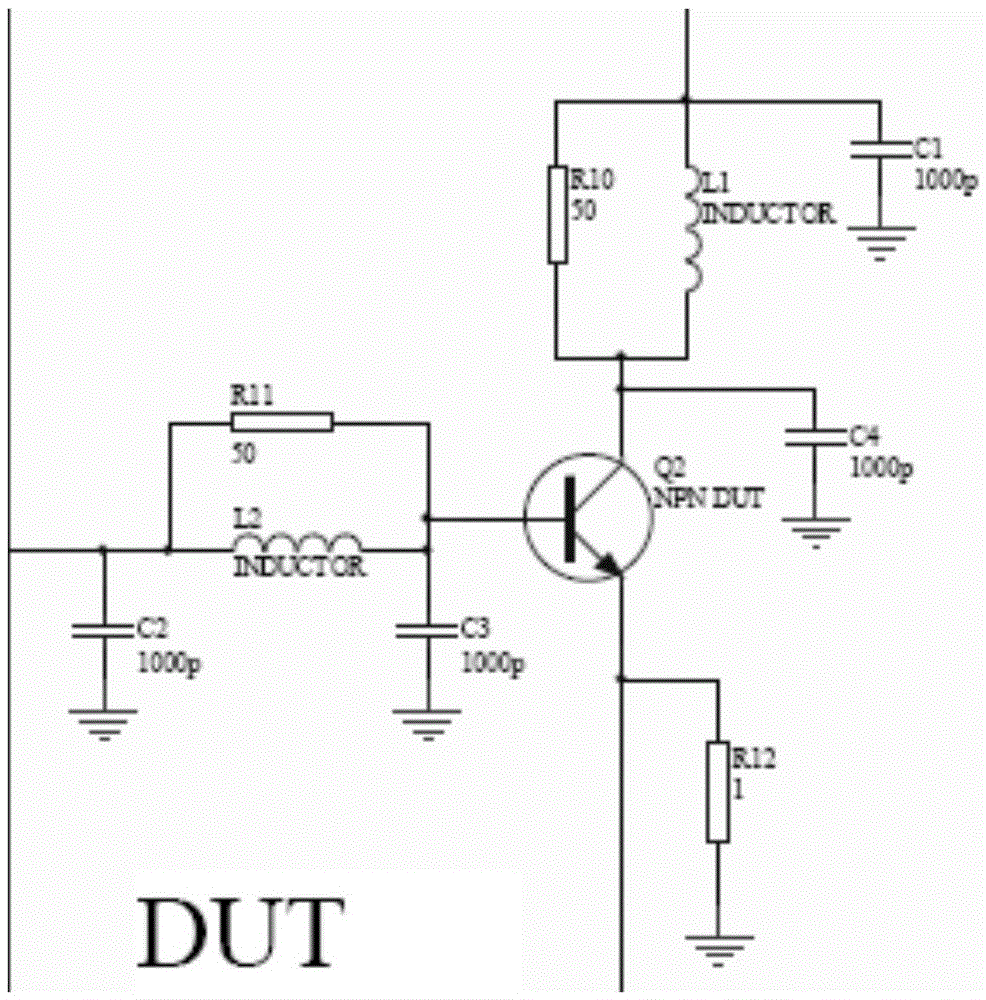
[0017] The specific implementation method of the present invention is as follows, the common emitter connection method is adopted for the B3 type transistor, and the common emitter connection method can effectively prevent the device from being damaged due to current overload, figure 2 Protection circuit for each transistor. Since the protection circuit must be close to the device to be effective, in addition, according to the position distribution of the heating hot hole 101 of the heating platform 102, each circuit board can be connected with 6 devices with protection circuits, and such 5 circuit boards are respectively fixed on the Above the heating platform, and the tube cap of the transistor is placed upside down in the heating hot hole 101, and thermal grease is applied to form a heating method of a hot plate. The heating platform 102 is a thick metal plate with a length, width and height of 230mm, 200mm and 60mm respectively, consisting of upper and lower layers, and h...


PUM


Abstract

The invention provides a transistor life test acceleration and operating point stabilization system and belongs to the field of the measuring technology and method. The transistor life test acceleration and operating point stabilization system comprises heating hot holes (101) which are used for placing devices, a heating platform (102), a temperature display (103), a power source biasing display (104) and a power source biasing controller (105); a main box (106) which is used for fixing the heating hot platform (102) is connected with a temperature controller (107); the number of the heating hot holes (101) which are in same shapes is 30; the heating hot holes (101) which are formed in the heating platform (102) can place B3 type packaging transistors. The transistor life test acceleration and operating point stabilization system can achieve a function of simultaneously heating and stabilizing working points of 30 transistors in same type.

Description

Technical field: [0001] Under the control of the PC, the invention realizes the real-time control of the operating points of several bipolar transistors, so that the operating points of the transistors are stabilized at the set value of the PC. As the internal parameters of the transistor (β, BVceo, etc.) and external conditions (tube temperature, etc.) When it is stable near the working point and the deviation is greater than the specified value, it will send out an audible and visual alarm. When the transistor is in an abnormal state, the transistor is protected in time to avoid damage to the transistor to the greatest extent. Background technique: [0002] In the military semiconductor devices of aerospace, aviation, ships, weapons and other weapons and equipment, the evaluation of new product identification, old product upgrade and reliability growth project needs to quantitatively give the life and failure rate of semiconductor devices. The values ​​of its life and fa...

Claims


Application Information

Patent Timeline
Patent Type & Authority Patents(China)
IPC IPC(8): G01R31/26G05D23/22
Inventor 张小玲谢雪松刘榿吕长志李志国
Owner BEIJING UNIV OF TECH
Why Eureka
Try Eureka