LED light source packaging structure

A technology of LED light source and packaging structure, which is applied in the direction of electrical components, electric solid devices, circuits, etc., can solve the problems of low heat dissipation capacity, resin aging, complex packaging process of LED light source module, etc., and achieve high heat dissipation efficiency

Active Publication Date: 2017-01-18
LEEDARSON IOT TECH INC
View PDF10 Cites 0 Cited by
  • Summary
  • Abstract
  • Description
  • Claims
  • Application Information

AI Technical Summary

Problems solved by technology

The existing 4πLED light source has a separate transparent substrate, and at the same time, the LED chip is packaged on the substrate and coated with a phosphor layer, there is a hidden danger of phosphor falling off, and the reliability is poor
At present, there are also packaging forms that use phosphor powder mixed with transparent resin. For example, the Chinese utility model patent with the authorized announcement date of November 27, 2013 and the authorized announcement number CN203309561U discloses a high-efficiency LED light source module, including transparent Substrate 1. An LED chip array is fixed on the transparent substrate 1. The LED chip array and the transparent substrate are integrally wrapped with a layer of encapsulating resin 3. The LED light source module formed by such encapsulation has a complicated encapsulation process, and has large thermal resistance and low heat dissipation capacity. Resin aging and other issues greatly affect and shorten the performance and service life of LED chips

Method used


Image

  • LED light source packaging structure
  • LED light source packaging structure
  • LED light source packaging structure

Examples


Embodiment Construction

[0013] The present invention will be further described in detail below in conjunction with the accompanying drawings and specific embodiments.

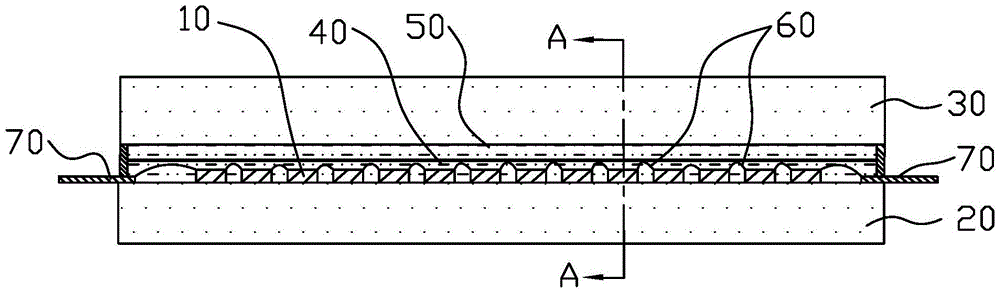
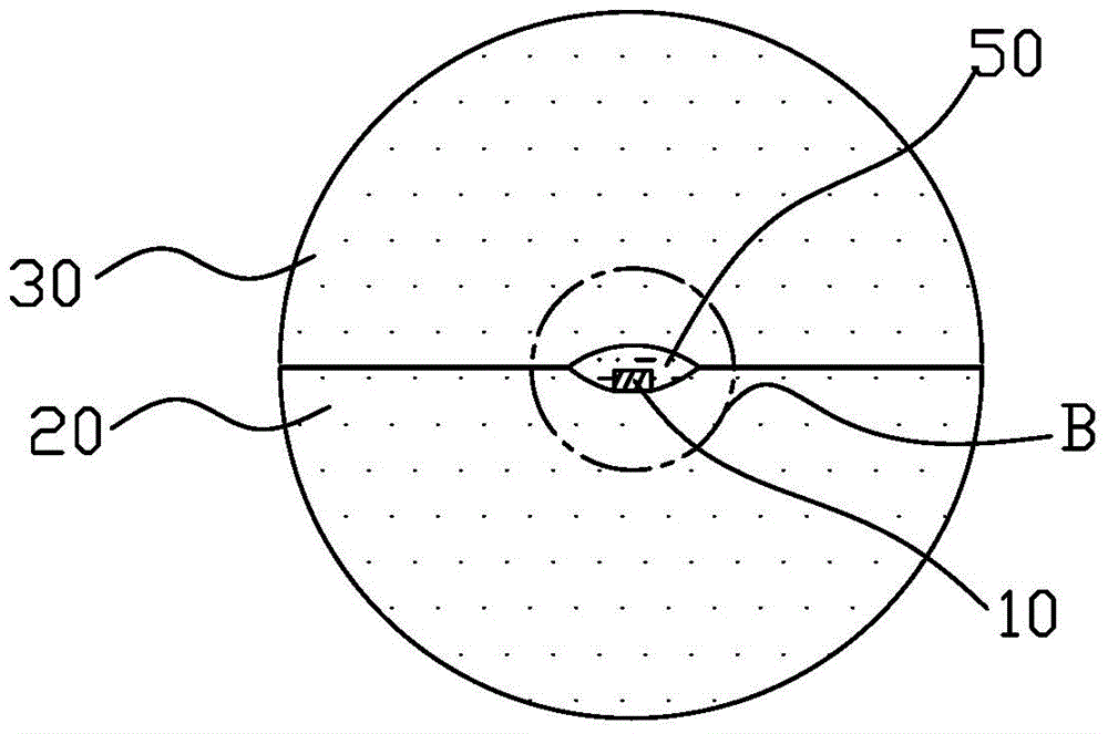
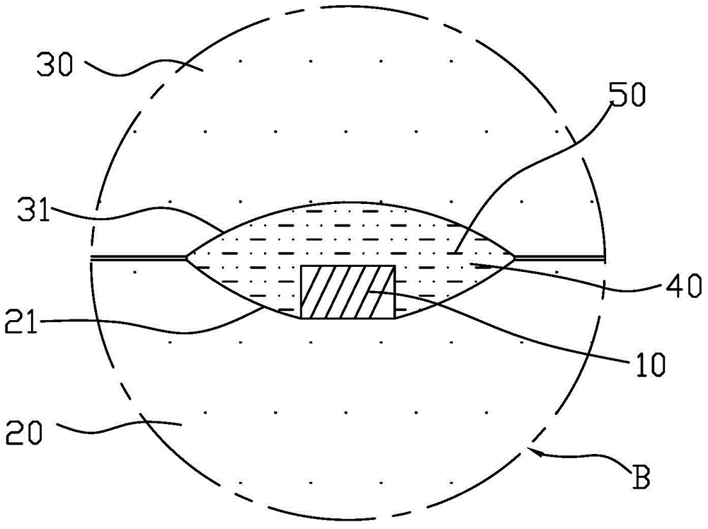
[0014] figure 1 It is a structural schematic diagram of the first embodiment of the packaging structure of the LED light source of the present invention. Please refer to figure 1 The LED light source packaging structure includes LED chips 10 , a base plate 20 and a cover plate 30 , these LED chips 10 are fixed on the base plate 20 , and these LED chips 10 are thermally connected to the base plate 20 .

[0015] Please refer to Figure 1 to Figure 3 The base plate 20 is integrally made of a transparent or translucent heat-conducting material mixed with phosphor powder. Preferably, the base plate 20 is made of phosphor powder and a transparent and highly thermally conductive inorganic material with good chemical compatibility and wettability with the phosphor powder. The bottom plate 20 is provided with a trapezoidal groove 21 (such a...


PUM


Abstract

The invention relates to an LED (Light-Emitting Diode) light source packaging structure, which comprises an LED chip, a bottom plate and a cover plate. The LED chip is fixedly arranged on the bottom plate. The cover plate covers the bottom plate. A holding tank is formed after the cover plate and the bottom plate are closed and is used for holding the LED chip. Transparent colloids are arranged in the holding tank to cover the LED chip. The LED chip is in hot connection with the bottom plate. The bottom plate is integrally made of a transparent or semi-transparent heat conducting material by mixing with fluorescent powder. The cover plate is made of a transparent or semi-transparent material and fluorescent powder is arranged on the cover plate at a position corresponding to the LED chip. The LED light source packaging structure not only can realize large-angle light emission, but also has the advantage of high heat dissipating efficiency.

Description

technical field [0001] The invention relates to the field of LED light sources, in particular to an LED light source packaging structure. Background technique [0002] LED light source is a green and environmentally friendly new light source. It has been widely used in the field of lighting. At present, there are many kinds of LED packaging structures in the market. At present, the packaging forms of 4πLED light source mainly include: one is to install the chip on a transparent substrate. Direct encapsulation; the second is to mount the chip on a transparent substrate, and then encapsulate it in a transparent device coated with a phosphor layer. Existing 4πLED light sources have separate transparent substrates, and at the same time, the LED chip is packaged on the substrate and coated with a phosphor layer, which may cause the phosphor to fall off and has poor reliability. At present, there are also packaging forms that use phosphor powder mixed with transparent resin. For ...

Claims


Application Information

Patent Timeline
Patent Type & Authority Patents(China)
IPC IPC(8): H01L25/075H01L33/48H01L33/50H01L33/64
Inventor 覃国恒郭伟杰李兆磊孔凡聪李永川
Owner LEEDARSON IOT TECH INC
Why Eureka
Try Eureka