A packaging structure and packaging method of a mems adjustable optical attenuator
A technology of dimming attenuation and packaging structure, which is applied in the coupling of optical waveguides, etc., can solve the problems of device cost increase and yield reduction, and achieve the effects of avoiding welding process, low cost and high reliability
- Summary
- Abstract
- Description
- Claims
- Application Information
AI Technical Summary
Problems solved by technology
Method used
Image
Examples
Embodiment Construction
[0047] The present invention will be further described below in conjunction with specific embodiment:
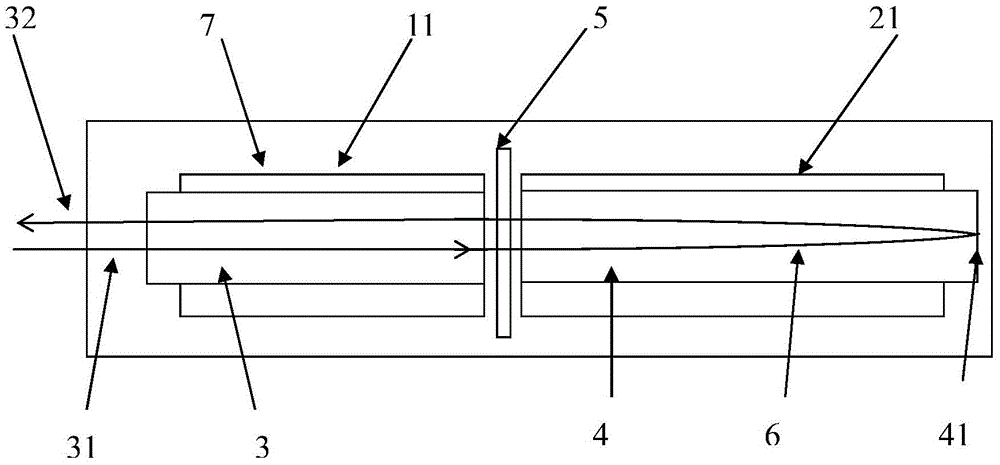
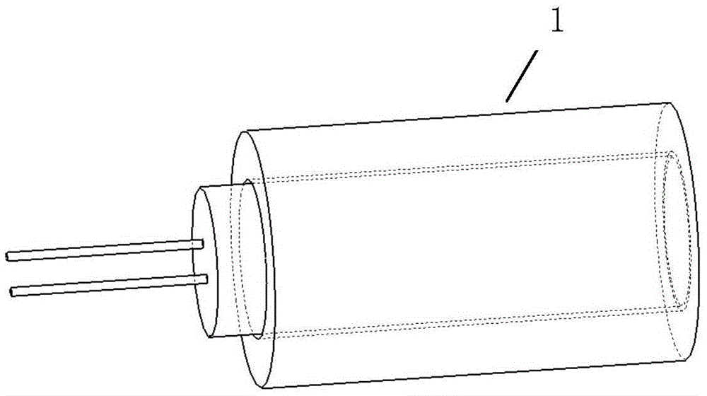
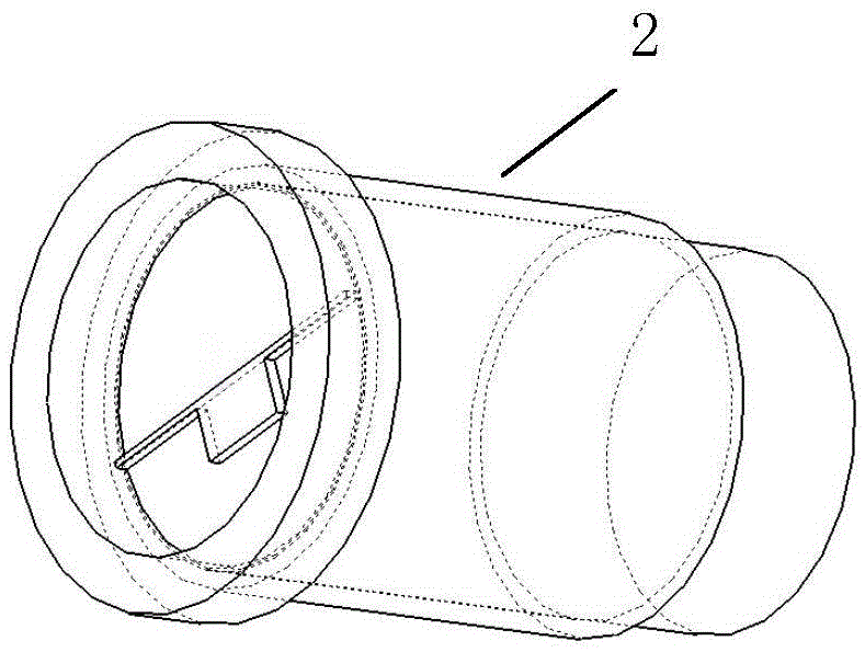
[0048] Such as figure 1 , figure 2 ,and image 3 As shown, a package structure of a MEMS tunable optical attenuator includes a focusing lens 4, a pigtail tube 3 with an input optical fiber 31 and an output optical fiber 32, and an optical chip 5 made by a micro-electromechanical system. The focusing lens is a self-focusing lens. The pigtail sleeve with input optical fiber and output optical fiber is fixed in the first hollow cylindrical magnet 11 with adhesive glue to form the first magnetic assembly 1; one end of the self-focusing lens is an optical signal incident surface, and the other end has a light reflection surface 41. Focusing lens light convergence point is located on light reflection surface 41; Self-focusing lens is fixed in the second hollow cylindrical magnet 21 with adhesive glue; The ends of the two hollow cylindrical magnets 21 for engaging with the fir...
PUM
 Abstract
Description
Claims
Application Information
 - R&D
- Intellectual Property
- Life Sciences
- Materials
- Tech Scout
- Unparalleled Data Quality
- Higher Quality Content
- 60% Fewer Hallucinations
Browse by: Latest US Patents, China's latest patents, Technical Efficacy Thesaurus, Application Domain, Technology Topic, Popular Technical Reports.
© 2025 PatSnap. All rights reserved.Legal|Privacy policy|Modern Slavery Act Transparency Statement|Sitemap|About US| Contact US: help@patsnap.com


