Embedded film resistor material and its preparation method
A thin film resistor, embedded technology, applied in the direction of coating resistance materials, resistors, non-adjustable metal resistors, etc.
- Summary
- Abstract
- Description
- Claims
- Application Information
AI Technical Summary
Problems solved by technology
Method used
Image


Examples
preparation example Construction
[0046] see figure 1 , the preparation method of the buried type thin film resistance material of one embodiment, comprises the following steps:
[0047] Step S110: providing a substrate.
[0048] The substrate is preferably a low profile flexible copper foil.
[0049] The substrate was ultrasonically cleaned in anhydrous acetone, anhydrous ethanol, and deionized water for 10 minutes each, then blown dry with a nitrogen gun, and then flattened with a clean glass plate for use.
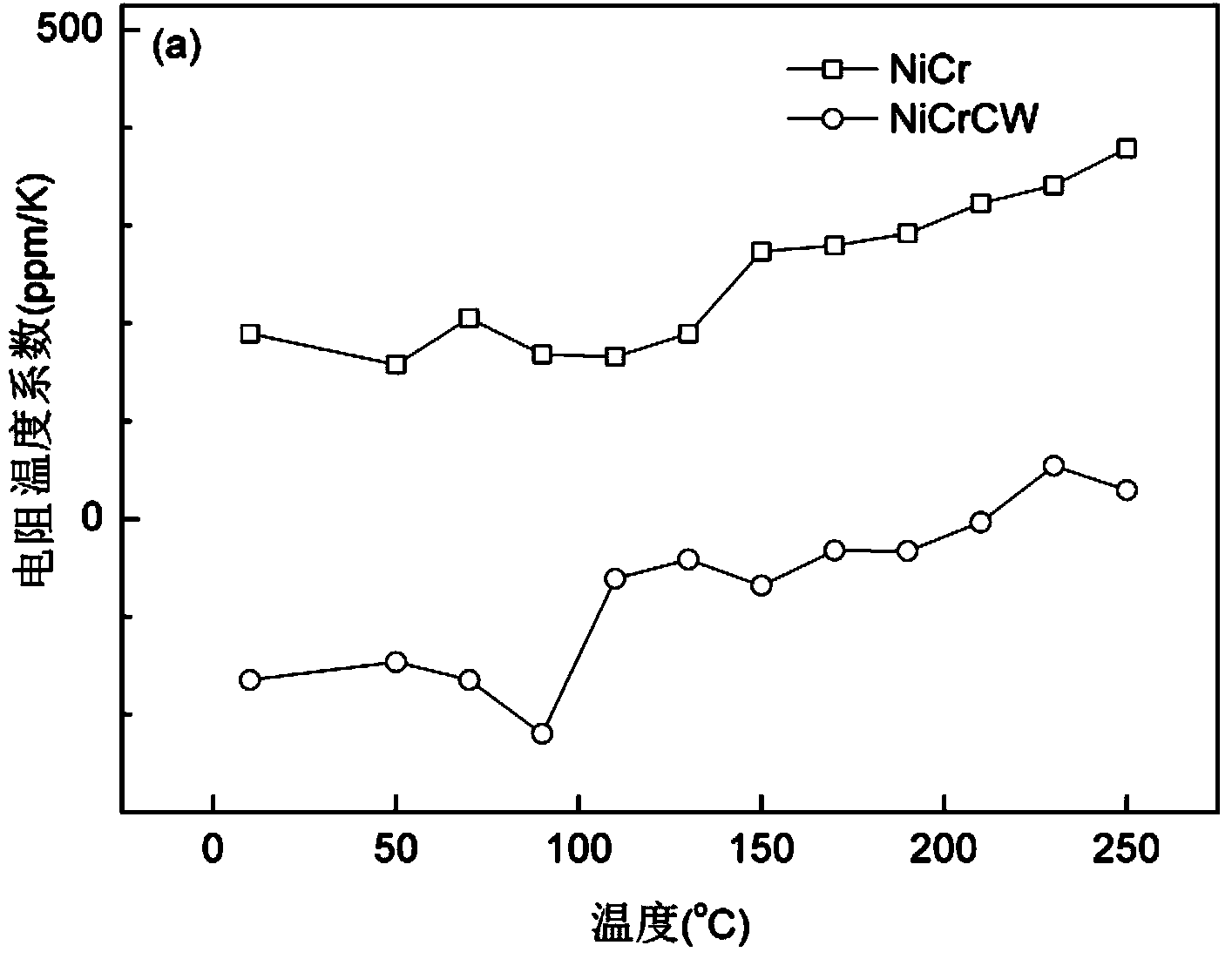
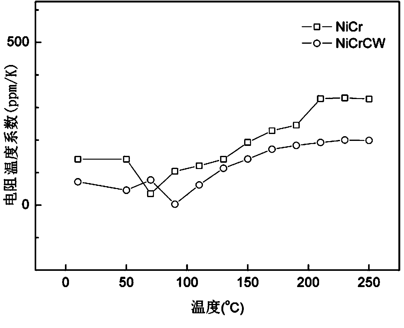
[0050] Step S120: Form a nickel-chromium-tungsten-carbon thin film on the substrate by sputtering to obtain an embedded thin-film resistance material, wherein the elements of the nickel-chromium-tungsten thin film include nickel 50-76%, chromium 10- 18%, carbon 10-30% and tungsten 0.5-5%.
[0051] Place the nickel-chromium alloy target (NiCr) in the cathode target position 1 of the vacuum sputtering chamber, the carbon target (C) in the cathode target position 2, and the tungsten target (W) in the cath...
Embodiment 1
[0069] Fabrication of embedded thin film resistor materials
[0070] (1) Ultrasonic clean the low-profile flexible copper foil with an area of 9cm×9cm in anhydrous acetone, anhydrous alcohol and deionized water for 10 minutes, then blow dry with a nitrogen gun, and then flatten it with a clean glass plate for use ;
[0071] (2) Place the flattened low-profile flexible copper foil on the rotating workpiece holder in the vacuum sputtering chamber, and close the vacuum sputtering chamber. Turn on the vacuum system, when the vacuum degree of the vacuum sputtering chamber reaches 4.0×10 -5 In the case of Tusla, argon gas is introduced, the gas flow rate is 25 sccm, the ionization power supply is started, and the surface of the substrate is ionized and cleaned for 10 minutes, and the sputtering power supply of the nickel-chromium alloy target, carbon target and tungsten target is immediately turned on. Sputter for 4 minutes to form a nickel-chromium-tungsten carbon film deposite...
Embodiment 2
[0074] Fabrication of embedded thin film resistor materials
[0075] (1) Ultrasonic clean the low-profile flexible copper foil with an area of 9cm×9cm in anhydrous acetone, anhydrous alcohol and deionized water for 10 minutes, then blow dry with a nitrogen gun, and then flatten it with a clean glass plate for use ;
[0076] (2) Place the flattened low-profile flexible copper foil on the rotating workpiece holder in the vacuum sputtering chamber, and close the vacuum sputtering chamber. Turn on the vacuum system, when the vacuum degree of the vacuum sputtering chamber reaches 4.0×10 -5 In the case of Tusla, argon gas is introduced, the gas flow rate is 25 sccm, the ionization power supply is started, and the surface of the substrate is ionized and cleaned for 10 minutes, and the sputtering power supply of the nickel-chromium alloy target, carbon target and tungsten target is immediately turned on. Sputtering for 4 minutes to form a nickel-chromium-tungsten carbon thin film ...
PUM
| Property | Measurement | Unit |
|---|---|---|
| Thickness | aaaaa | aaaaa |
| Thickness | aaaaa | aaaaa |
| Thickness | aaaaa | aaaaa |
Abstract
Description
Claims
Application Information
 - R&D
- Intellectual Property
- Life Sciences
- Materials
- Tech Scout
- Unparalleled Data Quality
- Higher Quality Content
- 60% Fewer Hallucinations
Browse by: Latest US Patents, China's latest patents, Technical Efficacy Thesaurus, Application Domain, Technology Topic, Popular Technical Reports.
© 2025 PatSnap. All rights reserved.Legal|Privacy policy|Modern Slavery Act Transparency Statement|Sitemap|About US| Contact US: help@patsnap.com