Imaging sensor packaging structure and method based on glass substrate

An image sensor and glass substrate technology, which is applied in the direction of electric solid-state devices, semiconductor devices, radiation control devices, etc., can solve the problem of parallelism between the sensing surface of the chip and the glass surface, affect the imaging performance of the CIS chip, and poor heat dissipation performance, etc. problems, to achieve improved thermal management performance, low cost, and good heat dissipation

Active Publication Date: 2014-02-12
NAT CENT FOR ADVANCED PACKAGING
View PDF3 Cites 6 Cited by
  • Summary
  • Abstract
  • Description
  • Claims
  • Application Information

AI Technical Summary

Problems solved by technology

[0002] At present, the traditional CIS (image sensor) packaging is usually packaged by wire bonding. There are some problems, such as the poor heat dissipation performance of the formed CIS packaging structure, which affects the imaging performance of the CIS chip. In addition, the traditional CIS packaging process The process faced in the process is relatively cumbersome
Moreover, due to the thickness control of the adhesive behind the CIS chip and the deviation when mounting the glass sheet used to protect the CIS chip during wire bonding packaging, the sensing surface of the chip in the CIS package is parallel to the glass surface. There is a problem

Method used


Image

  • Imaging sensor packaging structure and method based on glass substrate
  • Imaging sensor packaging structure and method based on glass substrate
  • Imaging sensor packaging structure and method based on glass substrate

Examples


Embodiment Construction

[0034] The present invention will be further described below in conjunction with specific drawings and embodiments.

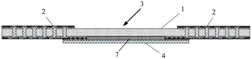
[0035] Such as Figure 1 to Figure 7 Shown: a glass substrate-based image sensor packaging structure, including a transparent glass substrate 1, the front and back of the glass substrate 1 are provided with wiring structures 2 and are electrically connected to each other; the glass substrate 1 has at least one The transparent area 3 without the wiring structure 2, the inverted image sensing chip 4 is mounted on the back of the glass substrate 1, and the sensing surface of the image sensing chip 4 faces the transparent area 3 of the glass substrate 1; the image sensing The chip 4 is electrically connected to the wiring structure 2 outside the transparent area 3 on the back of the glass substrate 1 ; The passive device 5 and the image sensor driver chip 6 are mounted on the front side of the glass substrate 1 other than the transparent area 3 and electrically co...


PUM


Abstract

The invention provides an imaging sensor packaging structure based on a glass substrate. The imaging sensor packaging structure comprises a transparent glass substrate, wiring structures are arranged on the front face and the back face of the glass substrate respectively and electrically connected mutually, at least one transparent area is arranged on the glass substrate and does not contain the wiring structures, inverted image sensing chips are attached to the back face of the glass substrate in a flip-chip bonding mode, and the sensing faces of the image sensing chips face toward the transparent area of the glass substrate; the image sensing chips are electrically connected with the wiring structures outside the transparent area on the back face of the glass substrate; heat sinks are fixed to the back faces of the image sensing chips; passive devices and image sensor driving chips are attached to the portion outside the transparent area on the front face of the glass substrate and electrically connected with the wiring structures of the front face; BGA welded balls are embedded into the area, where the wiring structures are located, of the back face of the glass substrate. The parallelism degree between the sensing faces of the image sensing chips and the glass substrate plane and the heat dissipation effect are better.

Description

technical field [0001] The invention relates to a packaging technology, in particular to a glass substrate-based image sensor packaging structure and packaging method. Background technique [0002] At present, the traditional CIS (image sensor) packaging is usually packaged by wire bonding. There are some problems, such as the poor heat dissipation performance of the formed CIS packaging structure, which affects the imaging performance of the CIS chip. In addition, the traditional CIS packaging process The process faced in the process is relatively cumbersome. Moreover, due to the thickness control of the adhesive behind the CIS chip and the deviation when mounting the glass sheet used to protect the CIS chip during wire bonding packaging, the sensing surface of the chip in the CIS package is parallel to the glass surface. There is a problem. Contents of the invention [0003] The purpose of the present invention is to overcome the deficiencies in the prior art, provide ...

Claims


Application Information

Patent Timeline
Patent Type & Authority Applications(China)
IPC IPC(8): H01L27/146H01L23/34
CPCH01L2924/0002
Inventor 郭学平宋见
Owner NAT CENT FOR ADVANCED PACKAGING
Why Eureka
Try Eureka