A kind of manufacturing method of sidewall metallization encapsulation product

A manufacturing method and metallization technology, applied in semiconductor/solid-state device manufacturing, electrical components, electric solid-state devices, etc., can solve the problems of reducing the number of packaging substrate units, increasing product quality risks, and increasing the cost of production tools to achieve packaging The effect of increasing the number of substrate units, reducing process complexity and production costs, and improving work efficiency

Active Publication Date: 2016-12-21
SKY CHIP INTERCONNECTION TECH CO LTD
View PDF10 Cites 0 Cited by
  • Summary
  • Abstract
  • Description
  • Claims
  • Application Information

AI Technical Summary

Problems solved by technology

Since the existing technology has carried out side wall metallization on the substrate before packaging, on the one hand, when performing packaging processes such as chip placement, wire bonding, package plastic sealing, and marking, vacuum adsorption technology is required, and When the substrate is metallized on the side wall, the slotted area is dense, which makes the shape of the substrate complex, so that special jigs need to be used to avoid the slotted area during the packaging process, and when using special jigs for vacuum adsorption, positioning Difficult, the process complexity is high and the work efficiency is low, and the use of special fixtures also increases the cost of production tools; , it is easy to cause the substrate to crack somewhere due to improper force application, thereby increasing the risk of product quality, especially for the case of thinner substrates and smaller-sized packaging substrate units, this problem is particularly prominent, and due to the groove It needs to occupy a large space, so that the number of packaging substrate units that can be laid out on a strip of a certain area is reduced

Method used


Image

  • A kind of manufacturing method of sidewall metallization encapsulation product
  • A kind of manufacturing method of sidewall metallization encapsulation product
  • A kind of manufacturing method of sidewall metallization encapsulation product

Examples


Embodiment Construction

[0027] It should be noted that, in the case of no conflict, the embodiments in the present application and the features in the embodiments can be combined with each other. The present invention will be further described in detail below in conjunction with the drawings and specific embodiments.

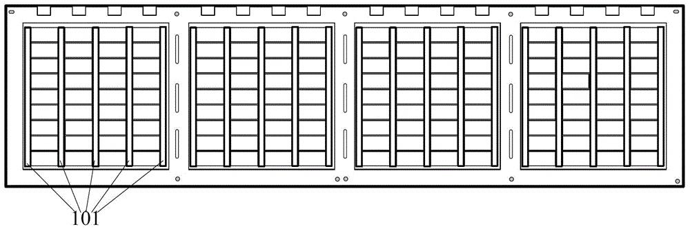
[0028] Before implementing the manufacturing method of a sidewall metallization packaging product according to the embodiment of the present invention, the following substrate structure is obtained through conventional substrate manufacturing and packaging processing: Figure 4 As shown, the substrate is composed of several packaging substrate units 401 , and circuits 402 are provided on the front and back sides of the packaging substrate units 401 .

[0029] Such as Figure 5 As shown, the manufacturing method of the above-mentioned sidewall metallization packaging product is mainly based on the above-mentioned substrate, and includes the following process flow:

[0030] 501 , make t...


PUM


Abstract

The embodiment of the present invention discloses a sidewall metallization method, which performs sidewall metallization treatment after packaging, and does not require slotting for sidewall metallization during substrate fabrication, which simplifies substrate fabrication. During the packaging process, due to The substrate has not been slotted for sidewall metallization, so that no special fixture is needed for vacuum adsorption technology, and the positioning is very simple, which simplifies the packaging process, thereby reducing the process complexity and production cost of sidewall metallization packaging products, and improving Improve work efficiency; when performing the above packaging process, because the substrate has not been slotted, the strength of the substrate is guaranteed, and the problem of cracking of the substrate will not be caused by improper force during packaging, thereby ensuring product quality. The accuracy is higher than the slotting accuracy during substrate fabrication, and the number of packaged substrate units that can be laid out on the strip increases. In addition, the processing method of the present invention can realize the processing of multi-electrode side wall metallization products.

Description

technical field [0001] The invention relates to the field of printed circuit boards, in particular to a method for manufacturing sidewall metallized packaging products. Background technique [0002] In the printed circuit board (Printed Circuit Board, PCB) or substrate (Substrate) manufacturing process, side wall metallization is to plate metal on the side of the package substrate unit, so as to realize the interconnection and conduction of the circuit on the front and back of the package substrate unit , and ensure good electrical performance and subsequent surface mount technology (Surface Mounted Technology, SMT) soldering reliability. Such as figure 1 As shown, a plurality of identical package arrays are usually arranged on a strip, and each package array is arranged with the same package substrate unit and electronic components arranged on each package substrate unit. There are grooves 101, and the strip will not be cut until the substrate of the entire strip is manuf...

Claims


Application Information

Patent Timeline
Patent Type & Authority Patents(China)
IPC IPC(8): H01L21/48H01L21/58
CPCH01L24/97H01L2224/48091H01L2224/48227
Inventor 李冠华江京彭勤卫
Owner SKY CHIP INTERCONNECTION TECH CO LTD
Why Eureka
Try Eureka