Discrete Carbon Nanotube Array Discharge Ionization Source
A carbon nanotube array and discrete technology, which is applied in the field of ionization sources, can solve the problems of difficult production, reduced ionization source stability, and easy corrosion, and achieves reduced stability, small space occupation, and low corrosion resistance. Effect
- Summary
- Abstract
- Description
- Claims
- Application Information
AI Technical Summary
Problems solved by technology
Method used
Image
Examples
Embodiment 1
[0026] The structure of the discrete carbon nanotube array discharge ionization source of the present invention is as follows figure 1 As shown, it includes a power supply, the power supply provides a voltage of 1.5-5kV, one end of the power supply is connected to the carbon nanotube array discharge electrode, and the other end is connected to the counter electrode, and the counter electrode can be a grid electrode or a ring electrode. A channel through which the sample passes is formed between the carbon nanotube array discharge electrode and the counter electrode. The carbon nanotube array discharge electrode includes a base layer, and a discrete needle point array is arranged on the base layer. Straight-length single carbon nanotubes.
[0027] Its working principle is as follows: the sample gas enters between the counter electrode and the carbon nanotube array discharge electrode from the discharge channel, and after the power supply reaches 2kV, the carbon nanotubes begin ...
Embodiment 2
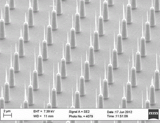
[0029] In the discrete carbon nanotube array discharge ionization source of the present invention, the base layer is preferably a silicon wafer, and a discrete needle tip array perpendicular to the silicon wafer is formed after deep reaction etching is adopted on the silicon wafer, so that The outer diameter of the discrete needle tip array is preferably 2 μm, the distance between the needle tip arrays is preferably 6 μm, and then single or multiple carbon nanotubes are vertically grown on the discrete needle tip array, Such as figure 2 Shown is a single carbon nanotube growing vertically; the radius of curvature of the end of the carbon nanotube is preferably 60 nm.
[0030] As other convertible implementations, the base layer can also be selected from other semiconductor materials, and the radius of curvature of the ends of the carbon nanotubes can also be selected between 20-90nm, and the radius of curvature in this range is larger than that of traditional The micron-leve...
Embodiment 3
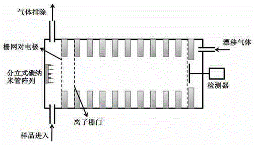
[0032] image 3 It is a structural diagram of the actual application of the discrete carbon nanotube array discharge ionization source described in the present invention to an ion mobility spectrometer, and its principle is as follows:
[0033] The sample gas enters the discrete carbon nanotube array discharge ionization source from the gas inlet, and ionization occurs to form ions. The sample ions enter the front of the ion gate under the action of the electric field. When the ion gate is opened, different types of ions are According to the difference of ion mobility, the detector will amplify the signal to obtain the sample spectrum.
PUM
 Abstract
Description
Claims
Application Information
 - R&D
- Intellectual Property
- Life Sciences
- Materials
- Tech Scout
- Unparalleled Data Quality
- Higher Quality Content
- 60% Fewer Hallucinations
Browse by: Latest US Patents, China's latest patents, Technical Efficacy Thesaurus, Application Domain, Technology Topic, Popular Technical Reports.
© 2025 PatSnap. All rights reserved.Legal|Privacy policy|Modern Slavery Act Transparency Statement|Sitemap|About US| Contact US: help@patsnap.com


