A method for manufacturing a drift region of a lateral high voltage device

A technology of lateral high voltage and manufacturing method, which is applied in the direction of semiconductor devices, electrical components, circuits, etc., can solve the problem of not being able to obtain high aspect ratio P-type strips, etc., to reduce the area of ​​the active area, reduce the specific on-resistance, and alleviate the contradiction relationship effect

Inactive Publication Date: 2016-04-06
UNIV OF ELECTRONICS SCI & TECH OF CHINA
View PDF3 Cites 0 Cited by
  • Summary
  • Abstract
  • Description
  • Claims
  • Application Information

AI Technical Summary

Problems solved by technology

At the same time, P-type strips and N-type strip structures with high aspect ratios cannot be obtained by general doping process

Method used


Image

  • A method for manufacturing a drift region of a lateral high voltage device
  • A method for manufacturing a drift region of a lateral high voltage device
  • A method for manufacturing a drift region of a lateral high voltage device

Examples


Embodiment Construction

[0031] Below in conjunction with accompanying drawing and embodiment, describe technical solution of the present invention in detail:

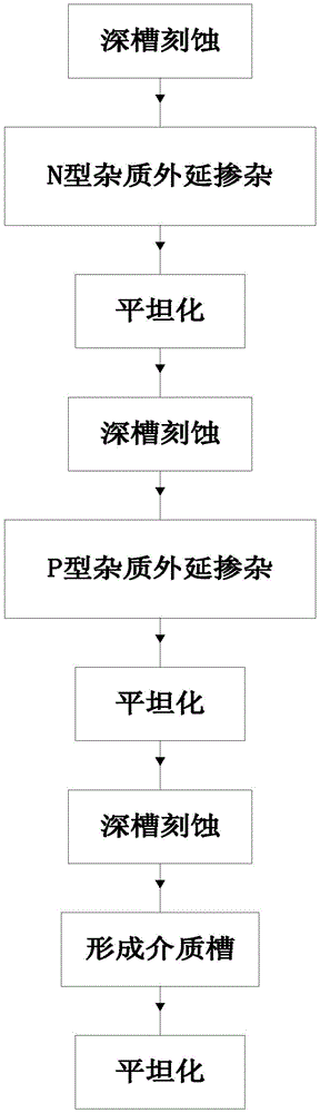
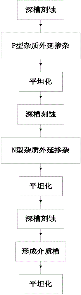
[0032] In the present invention, after obtaining the required deep and wide strip grooves by using etching technology in the drift region, the PN strip structure is obtained by epitaxial doping, and a dielectric groove with a specific width is added between the PN strips, and the depth of the dielectric groove is consistent with that of the PN strips. , using deposition or oxidation technology to fill the oxide dielectric groove, so as to obtain a withstand voltage structure that can manufacture the drift region of the lateral high voltage device. In the manufacturing process, by changing the width of the dielectric groove, the length of the drift region and the dopant dose, and then changing the concentration distribution of the PN bars, withstand voltage structures with different breakdown voltages can be obtained.

[0033] Such as figure 1...


PUM


Abstract

The invention relates to semiconductor technology, in particular to a process and manufacturing method for a voltage-resistant structure used in the drift region of a lateral high-voltage device. The main steps of the manufacturing method of the present invention are as follows: etching a first deep groove on the drift region of the lateral high-voltage device, filling the first deep groove and forming the impurity strip of the first conductivity type; Etching the second deep groove, filling the second deep groove and forming the second conductivity type impurity strip; etching the third deep groove on the drift region of the lateral high voltage device, filling the third deep groove with a medium to form a dielectric groove, Both sides of the dielectric groove are respectively connected with the impurity strips of the first conductivity type and the impurity strips of the second conductivity type. The invention has the beneficial effects of alleviating the contradictory relationship between the specific on-resistance and withstand voltage of the device, and forming a folded drift region in the dielectric groove, which can reduce the area of ​​the active region and significantly reduce the specific on-resistance. The invention is especially suitable for the manufacture of the drift region of the lateral high voltage device.

Description

technical field [0001] The invention relates to semiconductor technology, in particular to a process and manufacturing method for a voltage-resistant structure used in the drift region of a lateral high-voltage device. Background technique [0002] In order to achieve a high breakdown voltage, traditional power devices need to use a long drift region with a low doping concentration, which will increase the device area and lead to an increase in the specific on-resistance of the device. In order to shorten the length of the drift region of the device, shorten the length of the drift region through the withstand voltage of the trench oxide layer, and then reduce the specific on-resistance of the device, the "Ultra-lowSpecificOn-resistanceSOIHighVoltageTrenchLDMOSwithDielectricFieldEnhancementBasedonENBULFConcept" was published at the ISPSD conference in 2013, which proposed A slot-type drift region structure with N-type strips and P-type strips is proposed. Under reverse bias...

Claims


Application Information

Patent Timeline
Patent Type & Authority Patents(China)
IPC IPC(8): H01L29/06
CPCH01L29/0634
Inventor 乔明章文通薛腾飞祁娇娇张波
Owner UNIV OF ELECTRONICS SCI & TECH OF CHINA
Why Eureka
Try Eureka