Novel compound with electron injection and/or electron transport capabilities and organic light-emitting device including the same

An organic light-emitting device and electron transport technology, applied in organic chemistry, circuits, electrical components, etc., can solve the problems of anode delamination and poor durability, short lifespan of light-emitting devices, poor storage durability, etc.

Active Publication Date: 2014-01-29
SAMSUNG DISPLAY CO LTD
View PDF2 Cites 4 Cited by
  • Summary
  • Abstract
  • Description
  • Claims
  • Application Information

AI Technical Summary

Problems solved by technology

[0008] Conventional light-emitting devices using organic monomolecular materials for the electron transport layer have short lifetime, poor storage durability, and low reliability
These disadvantages are caused by physical changes, chemical changes, photochemical changes or electrochemical changes of organic materials and oxidation, delamination and poor durability of the anode

Method used


Image

  • Novel compound with electron injection and/or electron transport capabilities and organic light-emitting device including the same
  • Novel compound with electron injection and/or electron transport capabilities and organic light-emitting device including the same
  • Novel compound with electron injection and/or electron transport capabilities and organic light-emitting device including the same

Examples


example 1

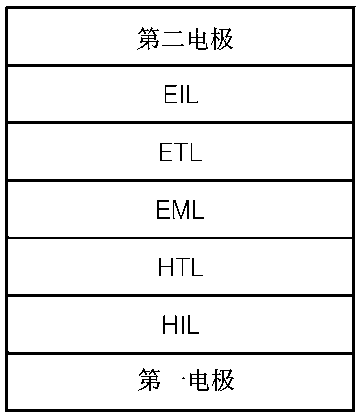
[0260] To make the anode, Corning15Ω / cm 2 The ITO glass substrate was cut into a size of 50 mm×50 mm×0.7 mm, then ultrasonically cleaned in both isopropanol and pure water for 5 minutes, and then cleaned by irradiating ultraviolet rays for 30 minutes and exposing to ozone. The obtained glass substrate was installed in a vacuum deposition apparatus.

[0261] Then, 2-TNATA as a HIL material was vacuum-deposited on the glass substrate to form a thickness of about The HIL. Then, 4,4′-bis[N-(1-naphthyl)-N-phenylamino]biphenyl (NPB) as a hole transport compound was vacuum-deposited on the HIL to form a thickness of about HTL.

[0262]

[0263] The blue fluorescent host 9,10-di-naphthalen-2-yl-anthracene (DNA) and the blue fluorescent dopant 1, both of which are well-known compounds, were co-deposited at a weight ratio of 98:2 on HTL. 4-bis-(2,2-diphenylvinyl)biphenyl (DPVBi) to form a thickness of EML.

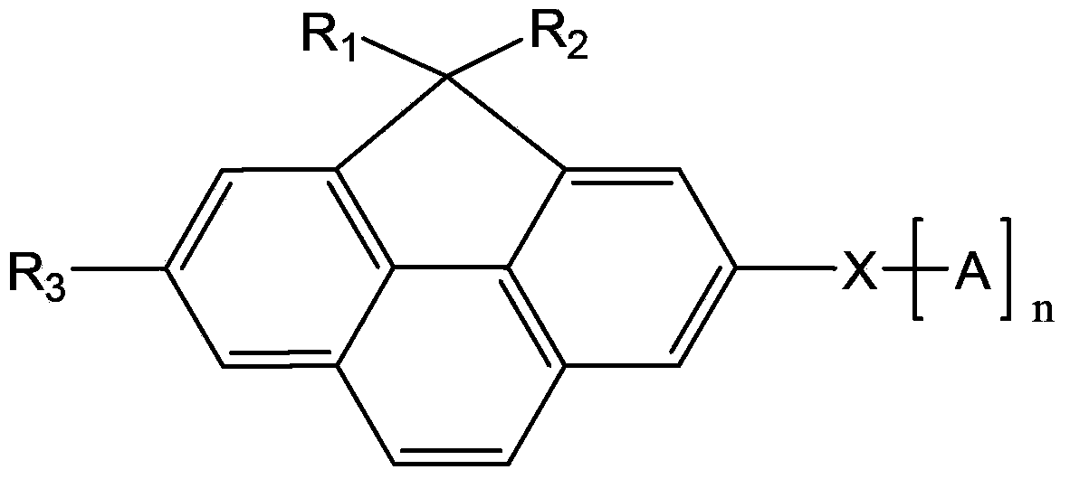
[0264] Then, compound 5 was deposited on the EML to form a thickn...

example 2

[0267] An organic light-emitting device was fabricated in the same manner as in Example 1, except that Compound 14 was used instead of Compound 5 to form the ETL.

[0268] The organic light-emitting device has a 50mA / cm 2 Drive voltage of about 5.31V, 2355cd / m 2 Luminosity, 4.71cd / A luminous efficiency and about 257 hours of half-life (hr100mA / cm 2 ).

example 3

[0270] An organic light-emitting device was fabricated in the same manner as in Example 1, except that Compound 32 was used instead of Compound 5 to form the ETL.

[0271] The organic light-emitting device has a 50mA / cm 2 Drive voltage of about 5.42V, 2240cd / m 2 The luminosity, the luminous efficiency of 4.48cd / A and the half-life of about 245 hours (hr100mA / cm 2 ).


PUM

PropertyMeasurementUnit
electric potential / voltageaaaaaaaaaa

Abstract

A compound represented by Formula 1 below and an organic light-emitting device including the compound are provided: Substituents in Formula 1 are the same as defined in the specification.

Description

[0001] Any and all applications on which foreign or domestic priority claims are based as indicated in the Application Data Sheet filed with this application are hereby incorporated by reference. [0002] This application claims the benefit of Korean Patent Application No. 10-2012-0075745 filed on Jul. 11, 2012 at the Korean Intellectual Property Office and No. 10-2013-0016979 filed on Feb. 18, 2013 at the Korean Intellectual Property Office Korean Patent Application No., the disclosure of which is hereby incorporated by reference. technical field [0003] One or more embodiments relate to a compound for an organic light emitting device and an organic light emitting device including the compound. Background technique [0004] Organic light-emitting devices (OLEDs), which are self-emitting devices, have advantages such as wide viewing angles, excellent contrast, fast response, high brightness, excellent driving voltage characteristics, and can provide multi-color images. [...

Claims


Application Information

Patent Timeline
Patent Type & Authority Applications(China)
IPC IPC(8): C07D213/06C07D215/06C07D251/24C07D235/18C07D401/10C07D487/04C07D401/14C07D417/10C07D413/10C07D471/04C07D409/14C07D405/14C07D213/22C07D401/04H01L51/54
CPCH01L51/0058H01L51/5072H01L51/0071H01L51/0062H01L51/0067H01L51/0054H01L51/0073H01L51/0072H01L51/0074C07D213/06C07D213/22C07D215/06C07D235/18C07D251/24C07D401/04C07D401/10C07D401/14C07D405/14C07D409/14C07D413/10C07D417/10C07D471/04C07D487/04H10K85/622H10K85/624H10K85/626H10K85/6565H10K85/615H10K85/654H10K85/657H10K85/6572H10K85/649H10K50/16H10K85/6574H10K85/6576
Inventor 郑惠珍黄皙焕金荣国林珍娱韩相铉郑恩在金秀娟朴俊河李银永李昌浩李钟赫
Owner SAMSUNG DISPLAY CO LTD
Why Eureka
Try Eureka