Power Clamp for esd protection between power supply and ground with dual channel technology

An ESD protection, dual-channel technology, applied in the field of clamping circuit and Powerclamp, can solve the problems of large layout area, waste, large capacitance and resistance, etc., and achieve the effect of reducing the layout area

Active Publication Date: 2017-03-29
南京文采工业智能研究院有限公司
View PDF7 Cites 0 Cited by
  • Summary
  • Abstract
  • Description
  • Claims
  • Application Information

AI Technical Summary

Problems solved by technology

[0006] For a general RC-triggered Power clamp, in order to achieve an effective discharge of the ESD current, the RC time constant needs to be designed to be 0.5us-1us. Such a large RC time constant requires relatively large capacitance and resistance. Therefore, when designing an integrated circuit layout, R and C require relatively large layout area, resulting in waste

Method used


Image

  • Power Clamp for esd protection between power supply and ground with dual channel technology
  • Power Clamp for esd protection between power supply and ground with dual channel technology

Examples


Embodiment Construction

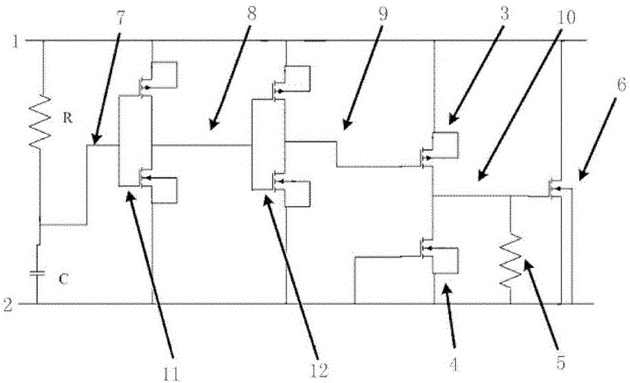
[0017] Such as figure 1 As shown, a Power Clamp using dual-channel technology for ESD protection between power and ground includes an RC trigger detection circuit between VDD (1) and VSS (2), and the detection circuit includes PMOS1 (3), NMOS1 (4), resistor R2 (5) and BigFET (6), and has Filter node ( 7 ), INV1OUT node ( 8 ), INV2OUT node ( 9 ) and BigFET gate node ( 10 ); R1 and C constitutes the ESD monitoring circuit, placed between VDD (1) and VSS (2), the inverter I (11) is placed after the RC monitoring circuit, the input terminal of the inverter I (11) and the Filter node (7) connected, the output terminal is connected to the inverter II (12), the output terminal of the inverter II (12) is connected to the gate of PMOS1 (3), the gate of NMOS1 (4) is grounded, the drain of NMOS1 (4) is connected to the gate of PMOS1 ( 3) The drain is connected to the gate of the BIGFET (6), and the gate of the BIGFET (6) is grounded through the resistor R2 (5).

[0018] Such as figure...


PUM


Abstract

The invention relates to a Power Clamp for ESD protection between a power supply and the ground by adopting a dual-channel technology. The adopted technical scheme is that the Power Clamp comprises an RC-triggered detection circuit, wherein R1 and C form an ESD monitoring circuit placed between VDD and VSS, a phase inverter I is placed behind an RC monitoring circuit, the input end is connected with a Filter node, and the output end is connected with a phase inverter II. The output end of the phase inverter II is connected with the grid of a PMOS1, the grid of an NMOS1 is grounded, the leakage of the NMOS1 is connected with the leakage of the PMOS1 and then connected with the grid of a BIGFET, and the grid of the BIGFET is simultaneously grounded through a resistor R. The Power Clamp adopts the dual-channel technology, an RC time constant only needs 10-50ns, and the layout area of the Power Clamp can be greatly decreased.

Description

technical field [0001] The invention relates to a Power Clamp that can be used for ESD protection between a power supply and a ground in a 65nm semiconductor process, in particular to an area-saving power clamp triggered by a resistor and a capacitor (clamping circuit between a power supply and a ground). Background technique [0002] Semiconductor processing technology enables the production of extremely small transistors. These tiny transistors have thin oxide insulating layers that are easily damaged by static electricity. Therefore, special care is required when handling these semiconductor devices. [0003] Electrostatic discharge (ESD, Electron Static Discharge) is an instantaneous process in which a large amount of static charge is poured into the integrated circuit from the outside to the inside when the pins of an integrated circuit are floating. The whole process takes about 100ns to 1us. When the electrostatic discharge of the integrated circuit will generate hu...

Claims


Application Information

Patent Timeline
Patent Type & Authority Patents(China)
IPC IPC(8): H02H9/04
Inventor 蔡小五高哲闫明梁超魏俊秀吕川
Owner 南京文采工业智能研究院有限公司
Why Eureka
Try Eureka