Method for repairing plasma damage in metal interconnection layer process

A technology of metal interconnection layer and ion body, which is applied in semiconductor/solid-state device manufacturing, electrical components, circuits, etc., can solve the problem of no repair of plasma damage, and achieve the effect of saving process steps

Inactive Publication Date: 2013-12-04
SHANGHAI HUALI MICROELECTRONICS CORP
View PDF4 Cites 3 Cited by
  • Summary
  • Abstract
  • Description
  • Claims
  • Application Information

AI Technical Summary

Problems solved by technology

[0005] It can be seen that there is still no method for repairing plasma damage during the subsequent metal interconnection layer production process.

Method used


Image

  • Method for repairing plasma damage in metal interconnection layer process
  • Method for repairing plasma damage in metal interconnection layer process
  • Method for repairing plasma damage in metal interconnection layer process

Examples


Embodiment Construction

[0025] The invention provides a method for repairing plasma damage in the metal interconnection layer process, which can be used in processes with technology nodes of 90nm, 65 / 55nm, 45 / 40nm, 32 / 28nm and less than or equal to 22nm; the invention can also be used in Logic , Memory, RF, HV, Analog / Power and other technology platforms.
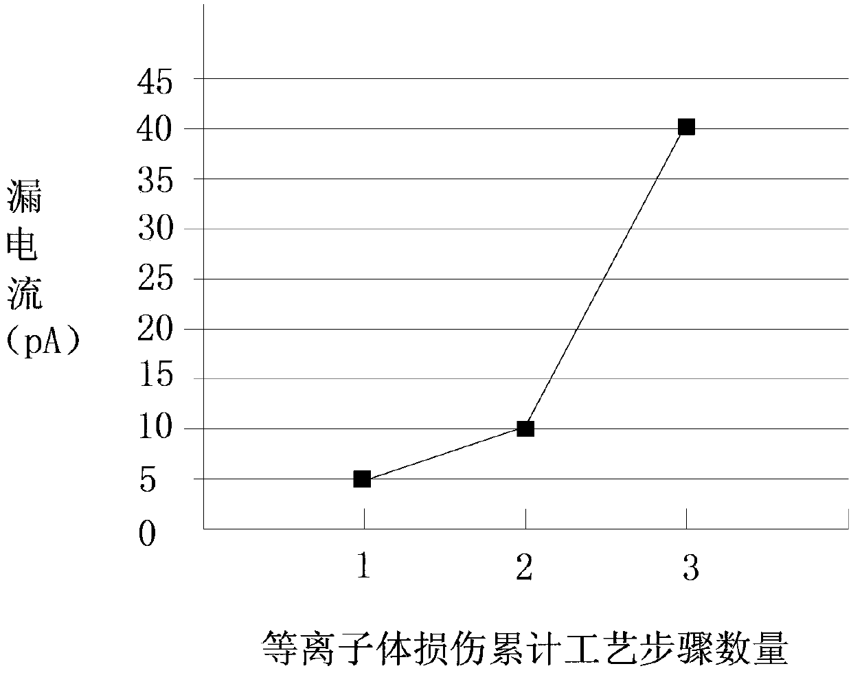
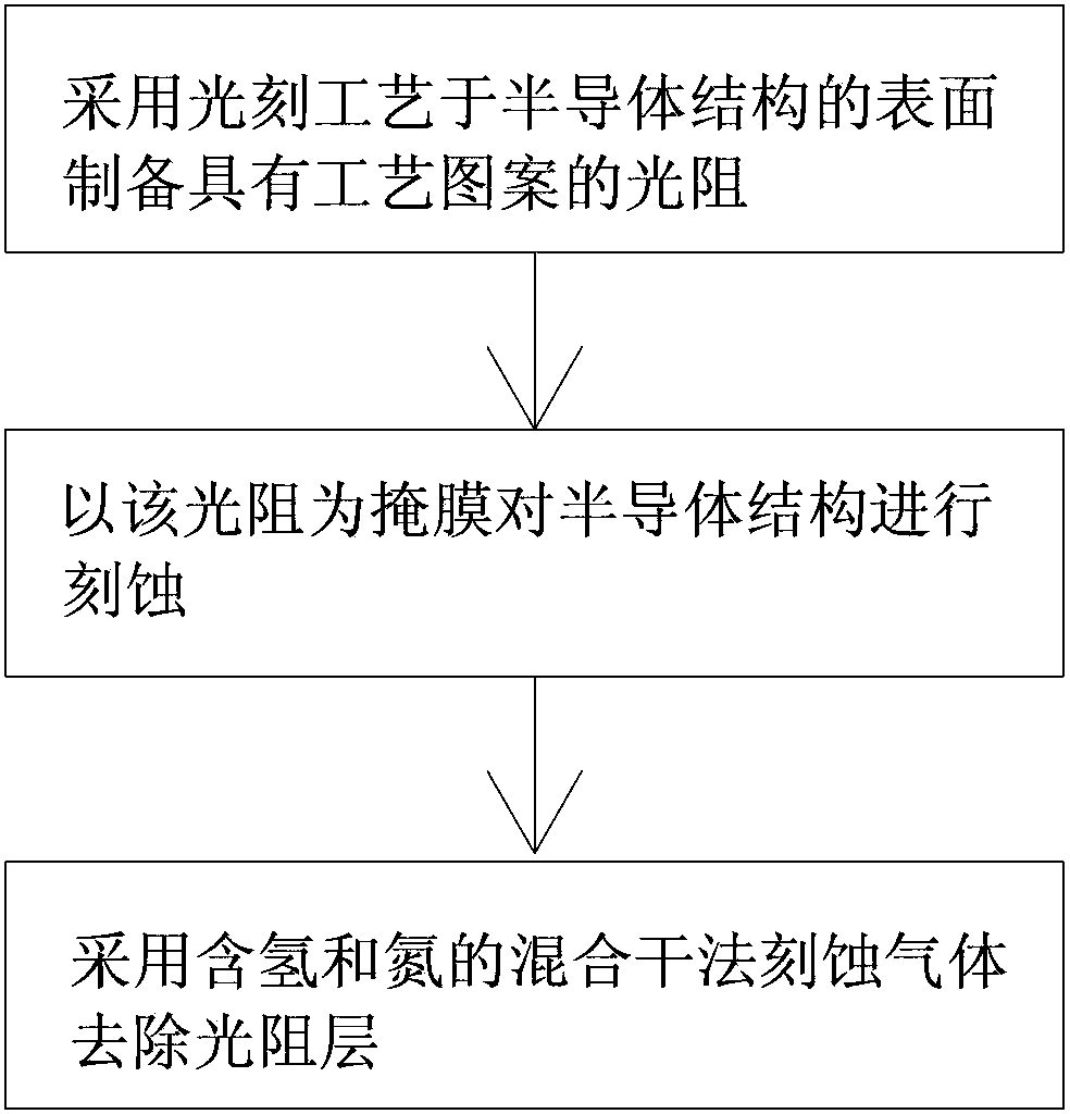
[0026] The main idea of ​​the present invention is to integrate the process step of repairing plasma damage into the etching step of removing the passivation layer of the top layer, not only does not add additional process steps, but also reduces the process of separate hydrogen annealing compared with the traditional process Steps simplify the process steps of the entire metal interconnection layer, and save process time while repairing plasma damage.

[0027] The method of the present invention specifically includes: during the production process of the metal interconnection layer, after the top passivation film is etched and removed, using a mi...


PUM


Abstract

The invention relates to a method for repairing plasma damage in a metal interconnection layer process. The method is applied to a semiconductor structure formed after a top passivating film deposition process in a preparation process of a rear metal interconnection layer. The method includes the steps: preparing a photo-resist layer with process patterns on the surface of the semiconductor structure by a photolithographic process; removing the photo-resist layer by mixed dry etching gas containing hydrogen and nitrogen after continuously etching the semiconductor structure by taking the photo-resist layer as a mask to repair the plasma damage in the semiconductor structure. The process effects of dry photo-resist removal and plasma damage repair can be simultaneously achieved only by one etching step. Compared with a traditional process, the method saves process steps.

Description

technical field [0001] The invention relates to a semiconductor manufacturing process method, in particular to a method for repairing plasma damage in the metal interconnection layer process. Background technique [0002] In the manufacturing process of semiconductor chips, the subsequent metal interconnection layer process includes film deposition, dry etching, chemical mechanical polishing and other processes. Among them, plasma enhanced chemical vapor deposition (PECVD for short) is used in the film deposition process; and etching needs to be performed under a high-power bias power supply in the through-hole etching process . The accumulation of plasma damage is unavoidable in the above two processes. When such ion damage defects accumulate to a certain extent, the charge breakdown effect will occur, causing damage to the device, such as figure 1 as shown, figure 1 is a schematic diagram of the relationship between plasma damage accumulation and device leakage perform...

Claims


Application Information

Patent Timeline
Patent Type & Authority Applications(China)
IPC IPC(8): H01L21/768
Inventor 荆泉任昱吕煜坤张旭昇
Owner SHANGHAI HUALI MICROELECTRONICS CORP
Why Eureka
Try Eureka