


Quick Research
Generate reliable direction feasibility study reports for your R&D in just a few steps.

Technical Q&A
Discover and master advanced knowledge NOW. Basics, ideas, possibilities, all at once.

Find Solutions
As an expert in R&D theories, this can generate solutions to your technical problems instantly.

Evaluate Feasibility
Analyze your overall solution with one click, know your potential R&D risks in advance.

Monitor Landscape
Get weekly tech updates, stay abreast of the latest tech innovations and key insights.
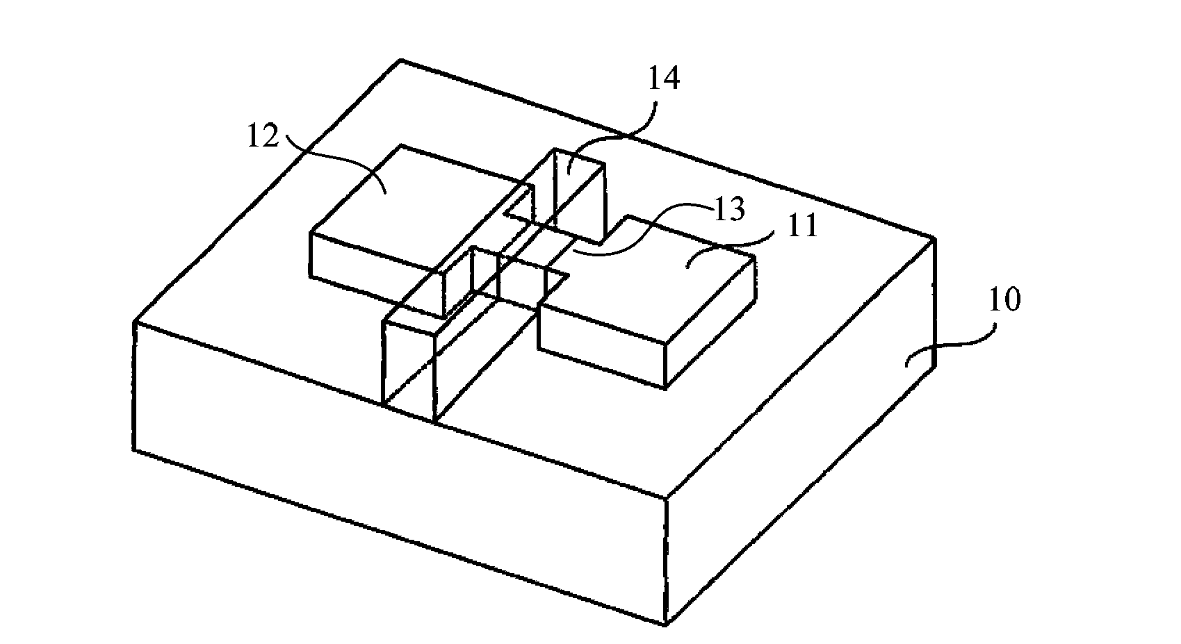
FinFET structure and manufacturing method thereof
A manufacturing method and gate structure technology, applied in semiconductor/solid-state device manufacturing, electrical components, circuits, etc., can solve the problems of not meeting the requirements of FinFET devices and limiting the performance of FinFET devices, so as to reduce the carrier scattering effect and improve Charge storage capacity, the effect of increasing the drive current
- Summary
- Abstract
- Description
- Claims
- Application Information
AI Technical Summary
Problems solved by technology
Method used
Image

Examples
Embodiment Construction
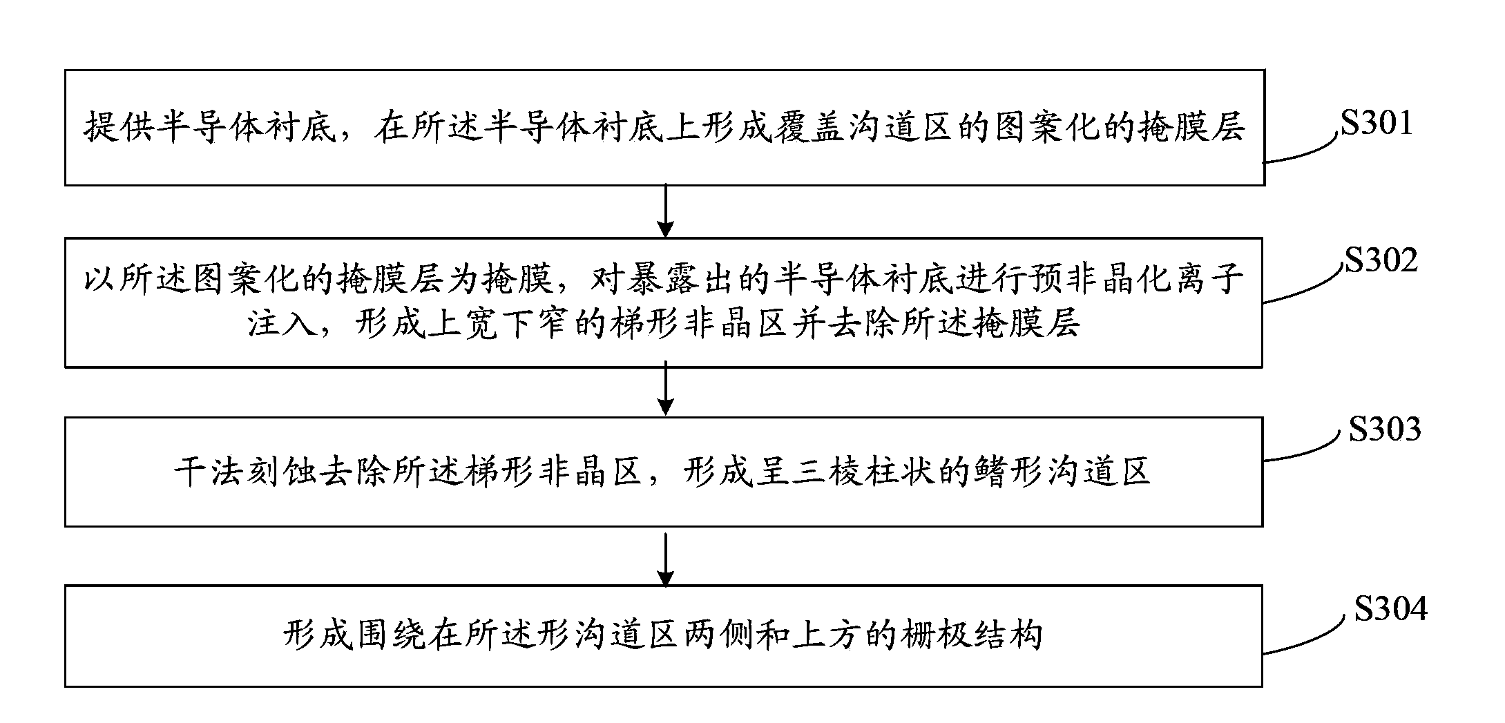
[0033] The FinFET structure and its manufacturing method proposed by the present invention will be further described in detail below in conjunction with the accompanying drawings and specific embodiments.
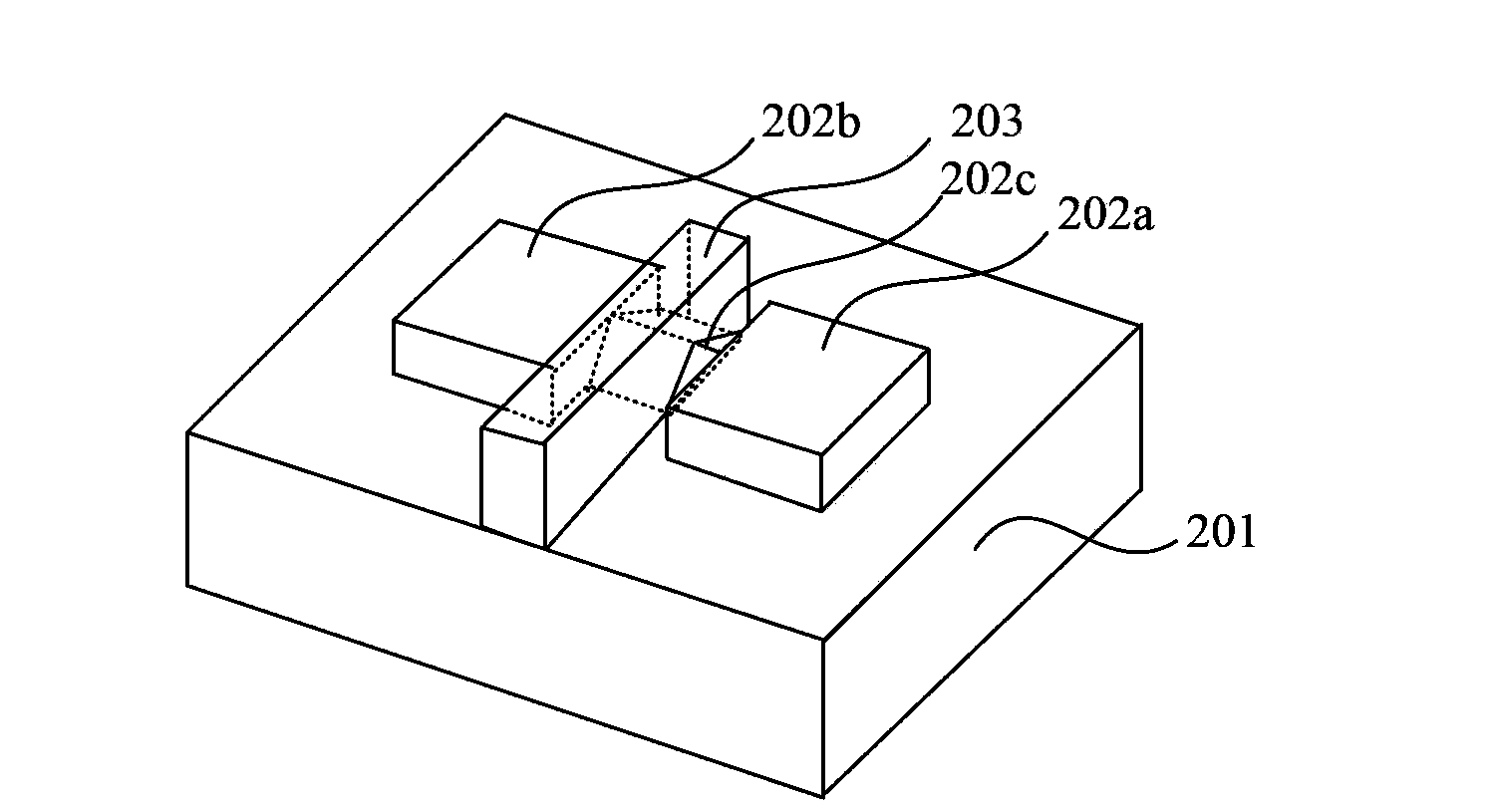
[0034] Such as figure 2 As shown, the present invention proposes a FinFET structure, including:
[0035] semiconductor substrate 201;
[0036] a source 202b and a drain 202a located on the semiconductor substrate;
[0037] a triangular prism fin-shaped channel region 202c located between the source 202b and the drain 202a; and,
[0038] The gate structure 203 surrounds the two sides and the top of the fin-shaped channel region 202c.
[0039] In this embodiment, the semiconductor substrate 201 is a silicon-on-insulator substrate or a silicon-germanium-on-insulator substrate.
[0040] Preferably, the bottom width of the fin-shaped channel region 202c is 5nm˜100nm. The fin-shaped channel region 202c of this size can be regarded as a nanowire. By making the lattice mismat...
PUM
| Property | Measurement | Unit |
|---|---|---|
| Bottom width | aaaaa | aaaaa |
| Thickness | aaaaa | aaaaa |
| Thickness | aaaaa | aaaaa |
Abstract
Description
Claims
Application Information
 - R&D Engineer
- R&D Manager
- IP Professional
- Industry Leading Data Capabilities
- Powerful AI technology
- Patent DNA Extraction
Browse by: Latest US Patents, China's latest patents, Technical Efficacy Thesaurus, Application Domain, Technology Topic, Popular Technical Reports.
© 2024 PatSnap. All rights reserved.Legal|Privacy policy|Modern Slavery Act Transparency Statement|Sitemap|About US| Contact US: help@patsnap.com