
Shallow trench isolation chemical-mechanical planarization method

A planarization method and chemical-mechanical technology, which is applied in the manufacture of electrical components, circuits, semiconductors/solid-state devices, etc., can solve problems such as device defects, large silicon oxide thickness drop, genetics, etc., to prevent excessive removal and improve uniformity Effect

Active Publication Date: 2013-10-30
INST OF MICROELECTRONICS CHINESE ACAD OF SCI
View PDF4 Cites 14 Cited by
  • Summary
  • Abstract
  • Description
  • Claims
  • Application Information

AI Technical Summary

Problems solved by technology

[0004] However, with the continuous increase of the depth of the shallow trench, after HDP-CVD, the silicon oxide thickness difference between the shallow trench isolation region and the non-shallow trench isolation region (active region or active region) becomes larger and larger. The larger the size, the greater the challenge for the next step Shallow Trench Isolation Chemical Mechanical Planarization (STI CMP) process to control the uniformity inside the wafer chip
Due to the large silicon oxide thickness drop (such as ), in the STI CMP process, the CMP abrasive will not only polish and remove the oxide on the top or peak, but also remove the oxide on the bottom or valley, so that this thickness drop cannot be directly eliminated by the CMP process, and will Inherited until the end of the CMP process
This causes part of the silicon oxide in the shallow trench to be worn away, forming dishing defects, which degrades the electrical performance of the device and even reduces the yield.
[0005] All in all, in the current STI manufacturing method, the large silicon oxide thickness difference reduces the uniformity of CMP and causes device defects

Method used


Image

  • Shallow trench isolation chemical-mechanical planarization method
  • Shallow trench isolation chemical-mechanical planarization method
  • Shallow trench isolation chemical-mechanical planarization method

Examples


Embodiment Construction

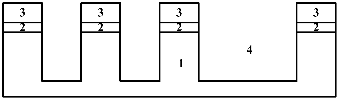
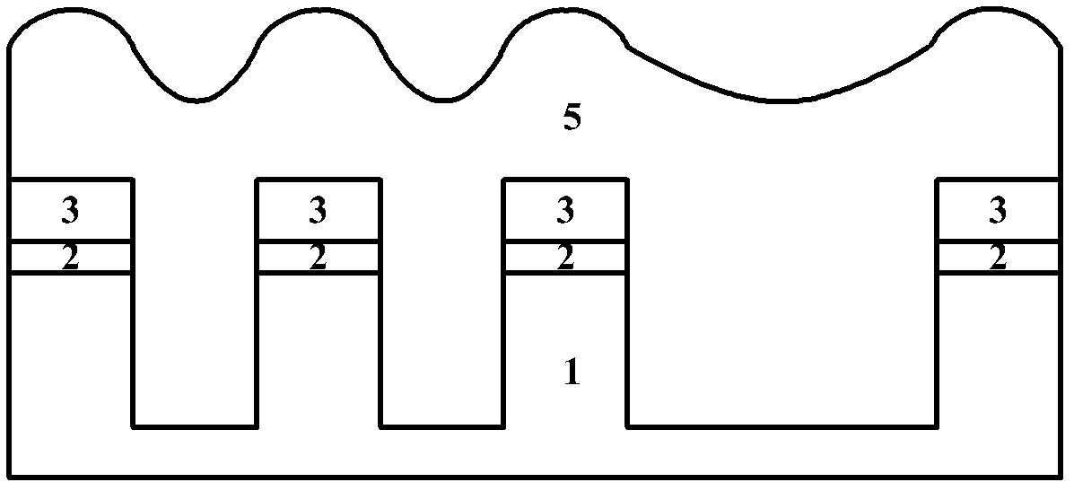
[0028] The features and technical effects of the technical solution of the present invention will be described in detail below with reference to the accompanying drawings and in conjunction with exemplary embodiments, and a shallow trench isolation chemical mechanical planarization method capable of improving step height uniformity is disclosed. It should be pointed out that similar reference numerals represent similar structures, and the terms "first", "second", "upper", "lower" and the like used in this application can be used to modify various device structures or manufacturing processes . These modifications do not imply spatial, sequential or hierarchical relationships of the modified device structures or fabrication processes unless specifically stated.

[0029] First, refer to figure 1 , forming a hard mask layer on the substrate. A substrate 1 is provided, such as bulk silicon, silicon-on-insulator (SOI), bulk germanium, germanium-on-insulator (GeOl), silicon germani...


PUM


Abstract

The invention discloses a shallow trench isolation chemical-mechanical planarization method which comprises the steps that hard mask layers are formed on a substrate; photoetching / etching is carried out on the hard mask layers to form hard mask patterns; the hard mask patterns serve as mask etching substrates to form shallow trenches; an isolation layer is deposited in the hard mask layers and the shallow trenches, wherein height differences exist among tops, in different areas, of the isolation layer; a conformal protective layer is formed on the isolation layer; chemical-mechanical planarization is carried out on the isolation layer and the protective layer until the hard mask layers are exposed. According to the shallow trench isolation chemical-mechanical planarization method, oxide locate in bottoms in shallow trench areas is prevented from being excessively removed by means of the protective layer additionally arranged on the top of the oxide, and therefore uniformity of step heights is effectively improved.

Description

technical field [0001] The invention relates to a semiconductor device manufacturing method, in particular to a shallow trench isolation chemical mechanical planarization method capable of improving step height uniformity. Background technique [0002] As the level of circuit integration is greatly improved, the spacing between various devices in the integrated circuit is gradually reduced, making parasitic effects, electromagnetic interference, etc. greatly hinder the improvement of device performance. In the previous large-scale process, a local field oxide layer was used between adjacent devices to provide isolation insulation. However, after the size of the device is reduced, the insulation performance of the oxide layer is reduced, and it is difficult to provide accurate patterns. Since the introduction of shallow trench isolation (STI) technology from the 0.25μm technology node, high-density isolation of devices has become possible. In addition, as technology nodes c...

Claims


Application Information

Patent Timeline
Patent Type & Authority Applications(China)
IPC IPC(8): H01L21/3105H01L21/762
Inventor 何卫朱慧珑
Owner INST OF MICROELECTRONICS CHINESE ACAD OF SCI
Learn More