Solar cell module based on glass conductive backboard and manufacturing method of solar cell module
A technology for solar cells and conductive back sheets, which is applied in the manufacture of electrical components, semiconductor devices, and final products, etc., can solve the problems of high cost and poor reliability, and achieve the effect of improving the reliability of use and avoiding the bending of the battery slices.
- Summary
- Abstract
- Description
- Claims
- Application Information
AI Technical Summary
Problems solved by technology
Method used
Image
Examples
Embodiment 1
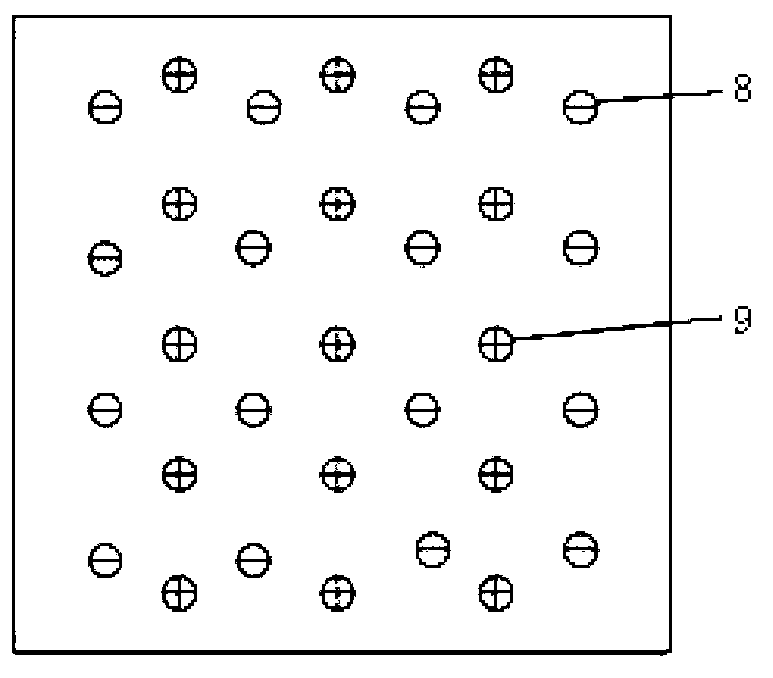
[0019] Embodiment 1: as figure 1 As shown, positive electrodes 9 and negative electrodes 8 are discretely distributed on the back of the existing MWT back contact battery. In the assembly production of such back contact cells, it is necessary to connect the positive electrode 9 with a conductor and the negative electrode 8 with another conductor.
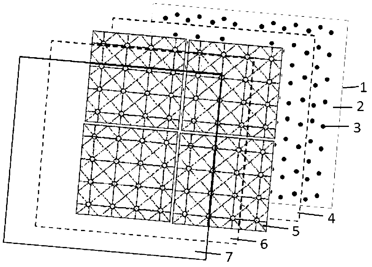
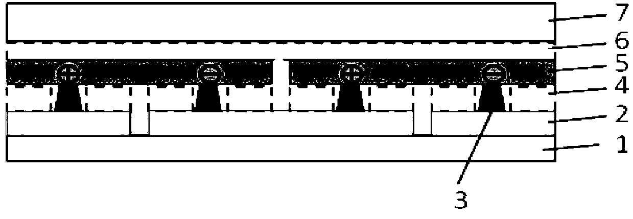
[0020] In this embodiment, a piece of ordinary silicate glass with a thickness of 2 mm and a warpage of 5 mm is selected as the glass back plate 1 . The glass backplane 1 is firstly cleaned on the surface, and then sent to thermal evaporation coating equipment for thermal evaporation coating of the aluminum film. During evaporation, the vacuum degree is controlled at 10 -3 Pa, the coating rate is 500nm / s, the total film thickness is 60um, and the time is two minutes. After the film coating is completed, the upper surface of the glass backplane 1 is covered with aluminum film. The aluminum film also needs to be processed into a p...
Embodiment 2
[0022]Embodiment 2: In this embodiment, the coating rate of the thermally evaporated aluminum film is 200 nm / s and the film thickness is 20 um on the glass backplane 1 with a thickness of 1 mm and a warpage of 1 mm. Then, a patterned aluminum film 2 is produced by using a sandblasting machine and a mask plate. The patterned aluminum film 2 is composed of strip-shaped aluminum strips, and the distance between two adjacent aluminum strips is 1mm. The stencil used for depositing the conductive adhesive connection point 3 on the patterned aluminum film 2 has a thickness of 100um and a circular hole diameter of 1mm. The height of the printed conductive glue connection point 3 is 100um. The conductive adhesive connection point 3 includes copper particles with a diameter of 1 um, and the copper particles are wrapped with a silver film to resist oxidation. After the conductive adhesive connection point 3 is printed, a layer of encapsulation film 4 is laid on the surface of the patter...
Embodiment 3
[0023] Embodiment 3: In this embodiment, the coating rate of the thermally evaporated aluminum film on the glass backplane 1 with a thickness of 3 mm and a warpage of 10 mm is 350 nm / s, and the film thickness is 40 um. Then, a patterned aluminum film 2 is produced by using a sandblasting machine and a mask plate. The patterned aluminum film 2 is composed of strip-shaped aluminum strips, and the distance between two adjacent aluminum strips is 3 mm. The stencil used for depositing the conductive adhesive connection point 3 on the patterned aluminum film 2 has a thickness of 500um and a circular hole diameter of 5mm. The height of the printed conductive adhesive connection point 3 is 500um. The conductive adhesive connection point 3 contains copper particles with a diameter of 20um, and the copper particles are wrapped with a silver film to resist oxidation. After the conductive adhesive connection point 3 is printed, a layer of encapsulation film 4 is laid on the surface of th...
PUM
 Abstract
Description
Claims
Application Information
 - R&D
- Intellectual Property
- Life Sciences
- Materials
- Tech Scout
- Unparalleled Data Quality
- Higher Quality Content
- 60% Fewer Hallucinations
Browse by: Latest US Patents, China's latest patents, Technical Efficacy Thesaurus, Application Domain, Technology Topic, Popular Technical Reports.
© 2025 PatSnap. All rights reserved.Legal|Privacy policy|Modern Slavery Act Transparency Statement|Sitemap|About US| Contact US: help@patsnap.com


