
Manufacturing method for separated grid type flash memory embedded into logical circuit

A manufacturing method and a technology of separating gates, which are applied in circuits, semiconductor/solid-state device manufacturing, electrical components, etc., can solve problems such as memory operating speed signal transmission bandwidth limitations, and achieve the effect of simplifying the manufacturing process

Active Publication Date: 2013-09-11
SEMICON MFG INT (SHANGHAI) CORP
View PDF3 Cites 9 Cited by
  • Summary
  • Abstract
  • Description
  • Claims
  • Application Information

AI Technical Summary

Problems solved by technology

If the split-gate flash memory, high-voltage circuit, and logic circuit are all built on a separate integrated chip, the operating speed of the entire memory will be limited by the signal transmission bandwidth between the flash memory and peripheral circuits

Method used


Image

  • Manufacturing method for separated grid type flash memory embedded into logical circuit
  • Manufacturing method for separated grid type flash memory embedded into logical circuit
  • Manufacturing method for separated grid type flash memory embedded into logical circuit

Examples


Embodiment Construction

[0034] The following describes the technical solutions of the present invention clearly and completely through specific embodiments in conjunction with the accompanying drawings. Obviously, the described embodiments are only a part of the implementation manners of the present invention, rather than all of them. According to these embodiments, all other implementation manners that can be obtained by a person of ordinary skill in the art without creative labor fall within the protection scope of the present invention.

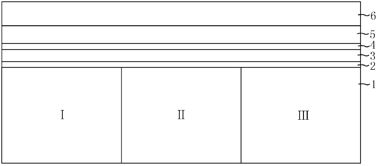
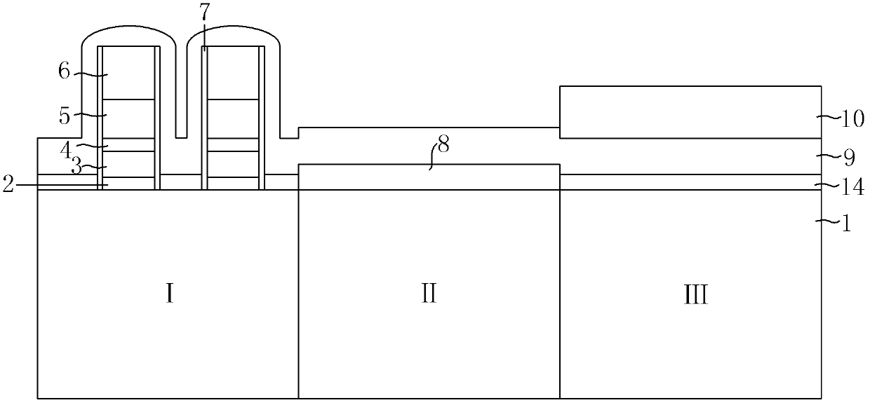
[0035] Figure 7 It is the manufacturing flow chart of the memory in the embodiment of the manufacturing method of the split-gate flash memory embedded in the logic circuit of the present invention, Figure 8 to Figure 19 Is in Figure 7 The schematic diagram of the structure of the split-gate flash memory embedded in the logic circuit during the manufacturing process is shown. The following will Figure 8 to Figure 19 versus Figure 7 The production method of the pr...


PUM


Abstract

The invention provides a manufacturing method for a separated grid type flash memory embedded into a logical circuit. According to the method, the separated grid type flash memory can be embedded into a peripheral circuit of a high-voltage circuit and the logical circuit, and the separated grid type flash memory, the high-voltage circuit and the logical circuit can be manufactured on a chip at the same time. After a stacking structure, comprising a floating gate oxide layer, a floating gate, a gate medium layer, a control gate and a hard mask layer, of the memory is formed, the thickness of a memory word line gate and the thickness of an erasing gate can be defined only through two-time polycrystalline silicon layer deposition and one-time photoetching glue line imaging treatment, and compared with three-time polycrystalline silicon layer deposition and two-time photoetching glue line imaging treatment in the prior art, the method greatly simplifies a manufacturing process. In addition, a gate medium layer of a high-voltage transistor is formed before the stacking structure of the memory is formed, and therefore the high-quality gate medium layer can be formed by means of a thermal oxidation growing method.

Description

Technical field [0001] The present invention relates to the field of semiconductor technology, in particular to a method for manufacturing a split gate type flash memory embedded in a logic circuit. Background technique [0002] Random access memory, such as DRAM and SRAM, has the problem of data loss after power failure during use. To overcome this problem, people have designed and developed a variety of non-volatile memories. Recently, flash memory based on the concept of a floating gate has become the most versatile nonvolatile memory due to its smaller cell size and good operating performance. The non-volatile memory mainly includes two basic structures: a stack gate structure and a split gate structure. Stacked gate memory includes a floating gate oxide layer formed on the substrate, a floating gate storing electrons, an oxide-nitride-oxide (ONO) stack structure and a control electron storage And release the control grid. The split-gate memory also includes a floating ga...

Claims


Application Information

Patent Timeline
IPC IPC(8): H01L21/8247
Inventor 刘艳周儒领
Owner SEMICON MFG INT (SHANGHAI) CORP
Learn More