
Nano-nickel rod array atomic force microscope tip characterization sample and its manufacturing method

An atomic force microscope and nanorod array technology, applied in scanning probe microscopy, scanning probe technology, measuring devices, etc., can solve the problems of poor consistency, high preparation cost, large size, etc., and reduce wear and preparation costs. Low, small feature size effect

Inactive Publication Date: 2016-08-10
FUZHOU UNIV
View PDF16 Cites 0 Cited by
  • Summary
  • Abstract
  • Description
  • Claims
  • Application Information

AI Technical Summary

Problems solved by technology

The preparation cost of MEMS characterization structure is too high, and the size is large, and its scale uncertainty will greatly affect the characterization of the tip of the AFM probe. In addition, this type of structure is easy to cause additional wear on the tip of the AFM probe. ; Nanostructures have a certain scale advantage in characterizing atomic force microscopy, but nanostructures have great randomness, poor consistency, and strict requirements for their feature sizes, and sometimes they need to be calibrated before they can be used

Method used


Image

  • Nano-nickel rod array atomic force microscope tip characterization sample and its manufacturing method
  • Nano-nickel rod array atomic force microscope tip characterization sample and its manufacturing method

Examples


Embodiment 1

[0034] (1) Wash the high-purity aluminum film with a purity of 99.99% in acetone solution for 20 minutes, infiltrate 5% NaOH solution for 7 minutes to remove the oxide layer on the surface of the aluminum film, rinse it with distilled water, and then perform annealing treatment;

[0035] (2) At 0°C, put the high-purity aluminum film obtained in the previous step into C 2 h 5 OH and HClO 4 Perform constant-pressure chemical polishing in the mixed solution for 8 minutes to remove the oxide layer on the surface of the aluminum sheet and improve the flatness of the surface;

[0036] (3) Put the polished high-purity aluminum film into the anodizing device for the first anodic oxidation, the first anodic oxidation is 5min, the oxidation is carried out under constant pressure conditions, and the PAA template obtained after the primary oxidation is immersed in 6%H 3 PO 4 and 1.8% H 2 CrO 4 In the mixed solution, place it at 60°C for more than 2.5 hours to dissolve the barrier l...


PUM

PropertyMeasurementUnit
diameteraaaaaaaaaa
thicknessaaaaaaaaaa
heightaaaaaaaaaa

Abstract

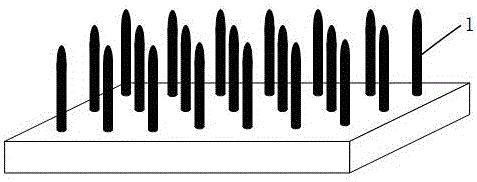
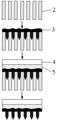
The invention relates to a nano-nickel rod array atomic force microscope tip characterization sample and a manufacturing method thereof. The method comprises the following steps of: using a secondary anodization method to obtain a porous alumina template by processing; by using an electron-beam evaporation based template synthesis method, evaporating nickel ions on the porous alumina template to form a nickel film; and fixedly supporting the nickel film with a nanorod array structure, removing the porous alumina template on the nickel film, and finally forming the nickel film with the nanorod array structure ( 1 ), i.e., the nano-nickel rod array atomic force microscope tip characterization sample. The method has a simple process and a low manufacturing cost, and the size, aspect ratio and density of the processed nano-nickel rod array structure can be realized by adjusting the structure of the porous alumina template, so that the nano-nickel rod array structure has larger degree of freedom. The nano-nickel rod array atomic force microscope tip characterization sample with small characteristic size, high aspect ratio and good consistency can be manufactured by the method.

Description

technical field [0001] The invention relates to the technical field of manufacturing an atomic force microscope tip characterization structure, in particular to a nano-nickel rod array structure that can be used as an atomic force microscope tip characterization sample and a manufacturing method thereof. Background technique [0002] The structure characterized by the tip of the traditional atomic force microscope mainly includes two categories: MEMS structure and nanostructure. The preparation cost of MEMS characterization structure is too high, and the size is large, and its scale uncertainty will greatly affect the characterization of the tip of the AFM probe. In addition, this type of structure is easy to cause additional wear on the tip of the AFM probe. ; Nanostructures have a certain scale advantage in the characterization of atomic force microscopy, but nanostructures have great randomness and poor consistency. There are strict requirements for their characteristic s...

Claims


Application Information

Patent Timeline
Patent Type & Authority Patents(China)
IPC IPC(8): G01Q60/38
Inventor 韩国强何炳蔚陈玉琴
Owner FUZHOU UNIV
Learn More