
Rapid frequency shift device and frequency shift method for semiconductor laser

A laser and semiconductor technology, applied in the direction of semiconductor lasers, lasers, laser components, etc., can solve the problems of high adjustment accuracy, high output optical power, and changes in fiber output power, and achieve optical power saving and large frequency shift range , the effect of reducing the demand for bandwidth

Active Publication Date: 2013-07-31
SHANGHAI INST OF OPTICS & FINE MECHANICS CHINESE ACAD OF SCI
View PDF3 Cites 20 Cited by
  • Summary
  • Abstract
  • Description
  • Claims
  • Application Information

AI Technical Summary

Problems solved by technology

However, this technology requires a large output optical power of the laser, and an optical amplifier is generally used, because the diffraction efficiency of the AOM is generally 60-80%, and the double-pass optical path produces two diffractions, which wastes a large amount of optical power in useless On the zero-order diffracted light, on the other hand, the coupling of spatial light into the optical fiber requires high adjustment accuracy of the optical path. At the same time, the diffraction efficiency of AOM changes with the frequency of the radio frequency, which will also cause a large change in the output power of the fiber. Therefore, This technology generally also requires optical power compensation; one method is a frequency-shift method based on the Zeeman effect (see prior art [4]: ​​"Frequency-shift of a frequency stabilized laser based on Zeeman effect", Chin. Phys .Lett.20,1714,2003), but the maximum frequency shifting speed and the maximum frequency shifting range of this method will be limited by several factors, so the prior technology achieves the fastest frequency shifting speed of about 1ms

Method used


Image

  • Rapid frequency shift device and frequency shift method for semiconductor laser
  • Rapid frequency shift device and frequency shift method for semiconductor laser

Examples


Embodiment Construction

[0018] The present invention will be further described below in conjunction with examples and accompanying drawings, but the protection scope of the present invention should not be limited thereby.

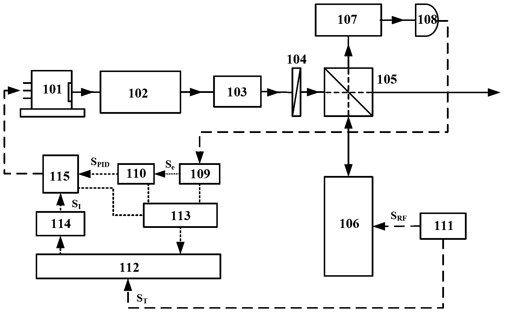
[0019] see first figure 1 , figure 1 It is a structural block diagram of the semiconductor laser fast frequency shifting device of the present invention. As can be seen from the figure, the composition of the device of the present invention includes a DBR laser 101, a shaping mirror 102, a Faraday isolator 103, a half-wave plate 104, a polarizing beam splitter 105, a double-pass AOM optical path 106, a saturated absorption optical path 107, a photodetector 108, Phase-locked demodulation circuit 109 , PID feedback circuit 110 , DDS signal generation circuit 111 , microcontroller 112 , analog-to-digital conversion circuit 113 , digital-to-analog conversion circuit 114 and laser current temperature control circuit 115 .

[0020] The positional relationship of the above-mentioned co...


PUM


Abstract

A rapid frequency shift device and method for a semiconductor laser. The device includes a DBR laser, a reshaping mirror, a Faraday isolator, a half wave plate, a polarization beam splitter, a bi-pass AOM optical path, a saturated absorption optical path, a photoelectric detector, a phase locking demodulator circuit, a PID feedback circuit, a DDS signal generation circuit, a microcontroller, an analog-digital conversion circuit, a digital-analog conversion circuit and a laser current temperature control circuit. According to the invention, the rapid frequency shift of the DBR laser can be realized while the locking state is kept, the bi-pass AOM optical path is applied in a frequency-stabilized optical path, so that the luminous power loss of the main optical path for cooling is greatly reduced; the frequency precompensation technology is adopted to realize rapid frequency shift and remarkably lower the requirement of the rapid frequency shift for system feedback bandwidth, and besides, the design difficulty of the feedback circuit is reduced, the design is changed to be simple, economic and easy to realize, so that the wide-range rapid tuning can be realized even though the feedback bandwidth is lower.

Description

technical field [0001] The invention relates to the field of photoelectric feedback control of semiconductor lasers, in particular to a semiconductor laser fast frequency shifting device and a frequency shifting method for atomic cooling. Background technique [0002] Atomic cooling technology can cool moving atoms to a very low temperature (uK or even nK level), at this time, some very important scientific experiments can be carried out, such as fine structure constant measurement, gravity field measurement, verification of general relativity and other sciences Research. The fountain atomic clock based on atomic cooling technology has gradually become a new generation of timekeeping standards due to its high precision, long-term continuous and stable operation and other excellent performance. , communications and other fields have significant applications. [0003] Atom cooling technology requires a frequency-stabilized laser light source with narrow linewidth and high fr...

Claims


Application Information

Patent Timeline
IPC IPC(8): H01S5/062
Inventor 孙延光董作人陈迪俊蔡海文瞿荣辉
Owner SHANGHAI INST OF OPTICS & FINE MECHANICS CHINESE ACAD OF SCI
Learn More