
Welding substrate for electronic product and manufacturing method of welding substrate

It is a technology for electronic products and substrates, which is applied in the direction of circuits, electrical components, and electrical solid devices. It can solve problems such as complex procedures, low precision of solder volume control, and low precision of chip welding positioning, achieving good flatness, high precision, Good welding performance

Active Publication Date: 2013-07-31
NO 43 INST OF CHINA ELECTRONICS TECH GRP CETC
View PDF8 Cites 7 Cited by
  • Summary
  • Abstract
  • Description
  • Claims
  • Application Information

AI Technical Summary

Problems solved by technology

[0003] In recent years, the optoelectronic communication market has shown a rapid growth trend, and the technical requirements are getting higher and higher. For example, in the field of high-end optical communication, the mounting and positioning accuracy of chips is required to be controlled at the micron level, and prefabricated solder and printing methods are used to prepare The accuracy of the solder pattern cannot be satisfied. The coating process and prefabricated solder can only produce alloys with a fixed ratio, and only thicker alloys can be produced. When installing the chip, the coating process must first manually coat the solder on the substrate, and then apply it For chip soldering, the process is complicated and the control accuracy of the amount of solder is low. The prefabricated solder has a low accuracy of the solder pattern due to the thick alloy solder, which leads to low soldering positioning accuracy of the chip.

Method used


Image

  • Welding substrate for electronic product and manufacturing method of welding substrate
  • Welding substrate for electronic product and manufacturing method of welding substrate
  • Welding substrate for electronic product and manufacturing method of welding substrate

Examples


Embodiment 1

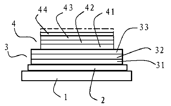
[0022] like figure 1 As shown, the electronic product welding substrate of the present invention comprises an alumina ceramic substrate 1, a metallized pattern layer 2 is provided on the substrate 1, and a gold-tin thin film layer 4 is arranged on the metallized pattern layer 2, and the gold-tin The thin film layer 4 is a multilayer structure in which gold layers and tin layers are alternately compounded and the uppermost layer is a gold layer. A barrier layer 3 is provided between the layer 4 and the metallized pattern layer 2. The barrier layer 3 is a three-layer metal layer structure, and the lower layer film 31 is composed of a tungsten-titanium alloy (WTi) layer, and a nickel-platinum-palladium layer. The middle film composed of alloy (NiPtPd) layer, the upper film composed of gold (Au) layer; the thickness of the tungsten-titanium alloy layer is 0.05-0.15 μm, the thickness of the nickel-platinum-palladium alloy layer is 0.2-1 μm, and the thickness of the gold layer is 0....

Embodiment 2

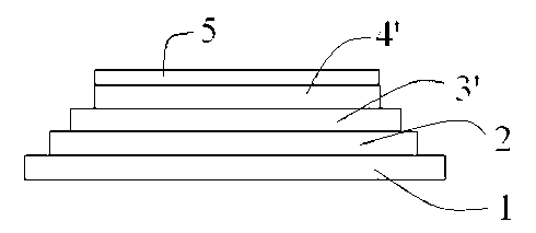
[0041] like figure 2 Shown, the welding substrate for electronic product of the present invention comprises alumina ceramic substrate 1, and substrate 1 is provided with metallized pattern layer 2, is provided with gold-tin film layer on this metallized pattern layer 2, and this gold-tin film layer The layer is a gold-tin alloy (AuSn) layer 4' with a thickness of 1.5-5 μm; a barrier layer is provided between the AuSn layer 4' and the metallized pattern layer 2, and the barrier layer is a platinum-palladium alloy (PtPd) layer 3', Layer thickness 0.5-1μm. The barrier layer of the present invention prevents the interdiffusion between the gold-tin film and the underlying metallization pattern layer during the soldering process. The gold-tin alloy layer 4' can adopt commonly used gold-tin components 70 / 30, 73 / 27 or 80 / 20; in order to make welding more effective, a gold layer is also provided on the entire area of ​​the gold-tin alloy layer 4' 5. The method described in Example ...


PUM

PropertyMeasurementUnit
thicknessaaaaaaaaaa
thicknessaaaaaaaaaa
thicknessaaaaaaaaaa

Abstract

The invention discloses a welding substrate for an electronic product. The welding substrate comprises a base plate, wherein the base plate is provided with a metallized graph layer, the metallized graph layer is provided with a gold-tin film layer, a barrier layer is arranged between the gold-tin film layer and the metallized graph layer and is a single metal film layer or a composite metal film layer, and the gold-tin film layer is a gold-tin alloy layer or is of a multi-layer structure formed by alternately compounding gold layers and tin layers. With the adoption of the film substrate, the graph line accuracy is high, the surface smoothness of the film layer is good, a chip can be directly welded and located without needing to precasting solders, the installation and locating accuracy of the chip can be ensured, and the film substrate is suitable for photoelectric products of high-power LED (light-Emitting Diode) optical communication and the like. Meanwhile, according to the film substrate disclosed by the invention, the proper component proportion of gold and tin in the film substrate can be adopted according to different chips needed to be welded on the underlay film substrate, so that the welding performance of the chips is better.

Description

technical field [0001] The present invention relates to the field of microelectronics and optoelectronic products, in particular to substrate substrates used for photoelectric communication, high-power lasers and LED circuit modules, soldering substrates for electronic products prepared by thin-film technology as solders, and soldering substrates for electronic products. Preparation. Background technique [0002] In the manufacturing process of high-power microelectronic devices, the function of the product is getting stronger, the integration is getting higher and higher, the size is getting smaller and smaller, the power density is getting higher and higher, and the heat dissipation problem is becoming more and more prominent and becomes the bottleneck of the product. Considering the large heat generated by the chip during operation, its structure needs to have a good heat dissipation channel, which is usually established by brazing the chip on the shell with a solder allo...

Claims


Application Information

Patent Timeline
Patent Type & Authority Applications(China)
IPC IPC(8): H01L23/488H01L23/14H01L21/48
CPCH01L23/4924H01L23/488H01L2224/29111H01L2224/29144H01L2224/2908H01L2924/0105
Inventor 汪涛李佳李林森宋泽润余传杰赵兹君陶允刚
Owner NO 43 INST OF CHINA ELECTRONICS TECH GRP CETC
Learn More