
Patsnap Eureka
For R&D, Patsnap Eureka makes reading and utilizing patents & technical documents easy.
Patsnap Eureka AIR
Designed for self-driven R&D workflows. Generate viable solutions, solve complex R&D challenges, empower your innovation with AI.

Patsnap Eureka Materials
Designed for material experts only. Revolutionize your material R&D, from search, analyze, to developing new materials.

TechResearch
Generate reliable direction feasibility study reports for your R&D in just a few steps.

TechSeek
Discover and master advanced knowledge NOW. Basics, ideas, possibilities, all at once.

TechMind
As an expert in R&D Theories, TechMind can generates customized viable solutions instantly.

TechRisk
Analyze your overall solution with one click, know your potential R&D risks in advance.

TechMonitor
Get weekly tech updates, stay abreast of the latest tech innovations and key insights.
An array substrate, its preparation method, and a display device
A technology of array substrates and substrates, which is applied in semiconductor/solid-state device manufacturing, electrical components, electric solid-state devices, etc., and can solve the problem that the aperture ratio is difficult to meet the demand
- Summary
- Abstract
- Description
- Claims
- Application Information
AI Technical Summary
Problems solved by technology
Method used
Image


Examples
preparation example Construction
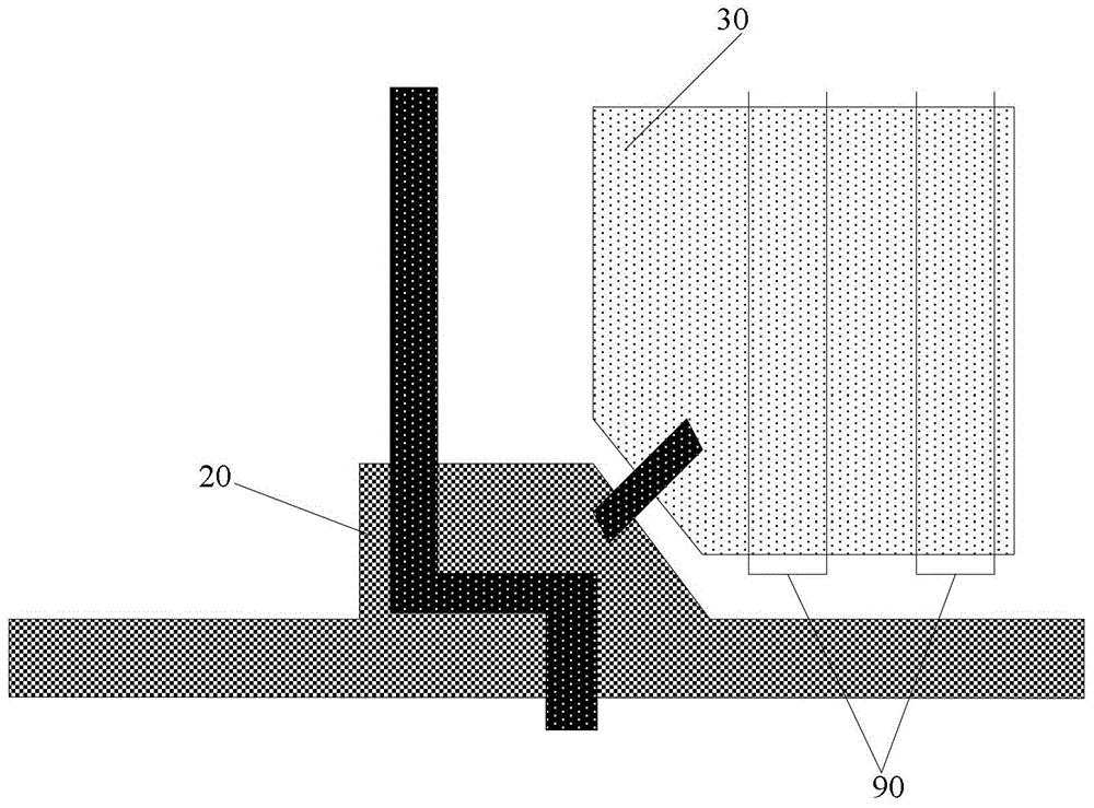
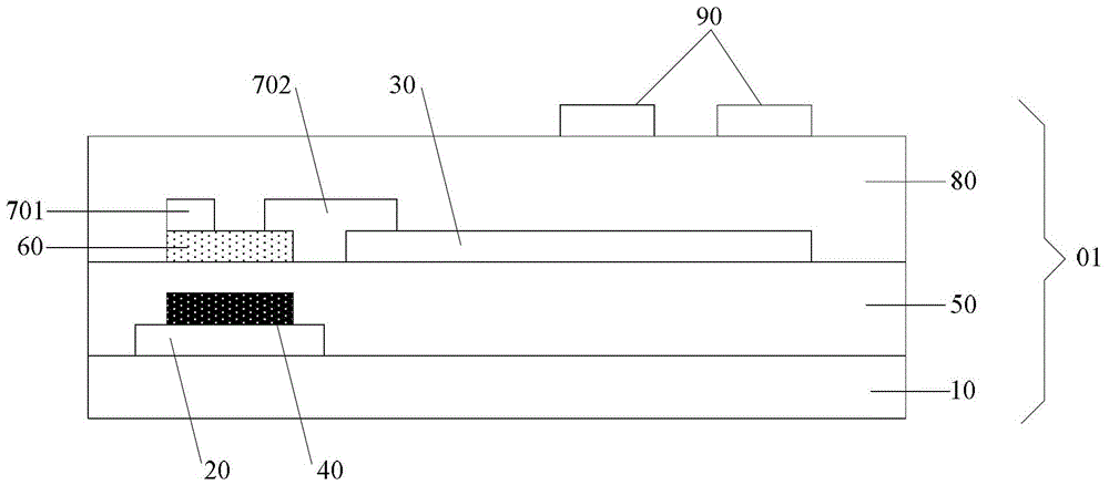
[0047] An embodiment of the present invention provides a method for preparing an array substrate, the method comprising: forming a thin film transistor and a pixel electrode 30 on the substrate, the thin film transistor including a gate electrode 20, a source electrode 701 and a drain electrode 702, and an active layer 60; further, the method further includes: forming a metal conductive region 40 above or below the gate electrode 20 for reducing the turn-on delay time of the thin film transistor.
[0048] The forming of the gate electrode 20 , the source electrode 701 and the drain electrode 702 on the substrate includes: forming the gate electrode 20 , the source electrode 701 and the drain electrode 702 of a transparent conductive material on the substrate.
[0049] An embodiment of the present invention provides a method for preparing an array substrate, the method comprising: forming a thin film transistor and a pixel electrode 30 on the substrate, the thin film transistor ...
Embodiment 1
[0064] Embodiment 1, the embodiment of the present invention provides a method for preparing a bottom-gate array substrate, such as Figure 7 shown, including the following steps:
[0065] S101. Fabricate a transparent conductive film on the substrate 10, and form a patterning process such as Figure 8 Gate electrode 20 and pixel electrode 30 are shown.
[0066] Specifically, chemical vapor deposition can be used to deposit a layer with a thickness of arrive The transparent conductive film layer between, wherein commonly used transparent conductive film can be ITO or IZO thin film; Then coat one deck photoresist on described transparent conductive film, and utilize promptly to comprise grid electrode 20 patterns and comprise pixel electrode 30 again The patterned mask board exposes the substrate on which the photoresist is formed, and after developing and etching, the gate electrode 20 and the pixel electrode 30 are formed on a certain area of the substrate. Of course,...
Embodiment 2
[0092] Embodiment 2, the embodiment of the present invention provides a method for preparing a bottom-gate array substrate, such as Figure 14 shown, including the following steps:
[0093] S201. Fabricate a transparent conductive film on the substrate 10, and form such a pattern through a patterning process. Figure 15 The gate electrode 20 is shown.
[0094] Of course, here, while forming the gate electrode 20 , the gate lines and gate line leads electrically connected to the gate electrodes 20 are also formed.
[0095] S202. On the substrate that has completed step S201, make a metal conductive film, and form a metal conductive film on the gate electrode 20 through a patterning process. Figure 16 The metal conductive region 40 is shown, and the metal conductive region 40 corresponds to the active layer 60 to be formed in the following step S204.
[0096] Here, the formation position of the metal conductive region 40 needs to be determined according to the formation posi...
PUM
 Abstract
Description
Claims
Application Information
 - R&D Engineer
- R&D Manager
- IP Professional
- Industry Leading Data Capabilities
- Powerful AI technology
- Patent DNA Extraction
Browse by: Latest US Patents, China's latest patents, Technical Efficacy Thesaurus, Application Domain, Technology Topic, Popular Technical Reports.
© 2024 PatSnap. All rights reserved.Legal|Privacy policy|Modern Slavery Act Transparency Statement|Sitemap|About US| Contact US: help@patsnap.com