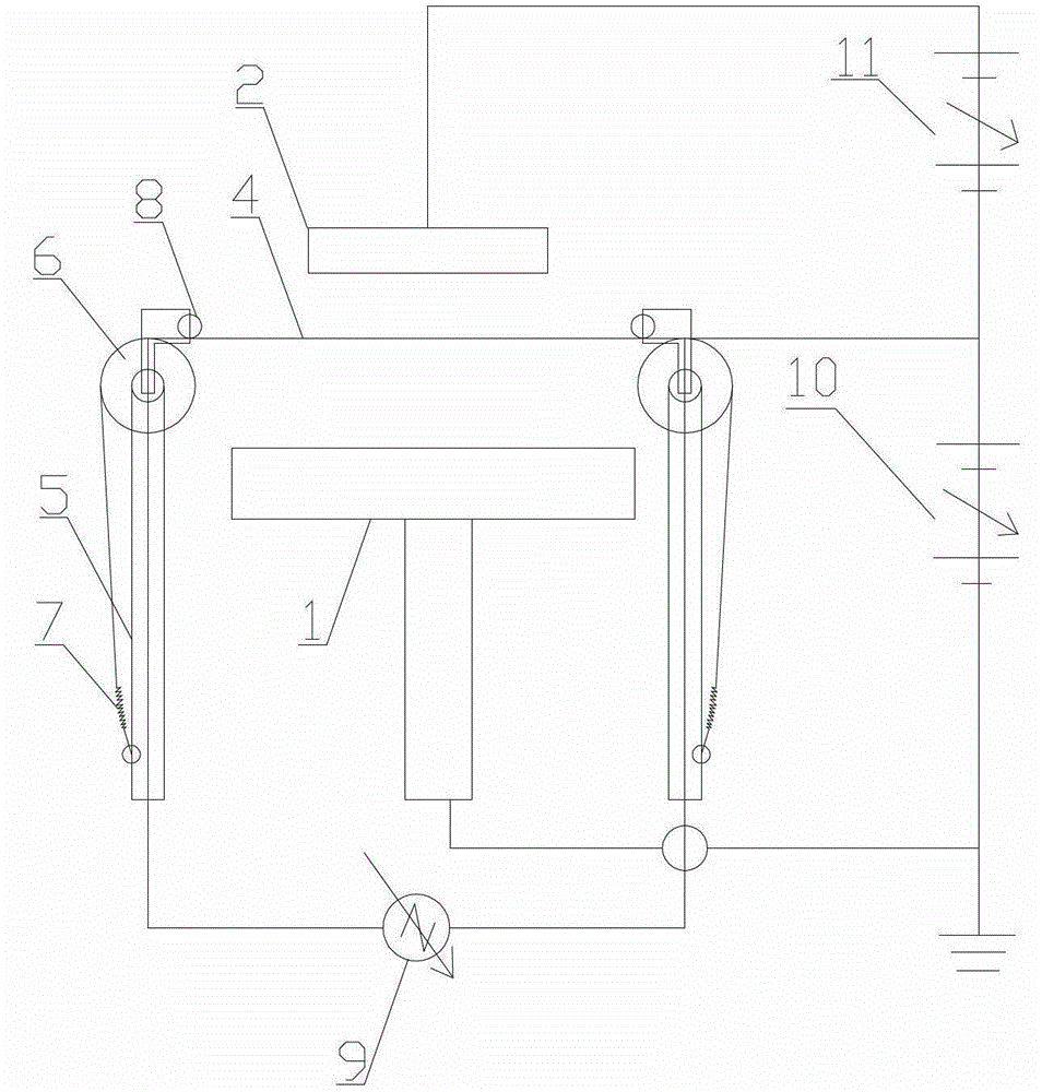
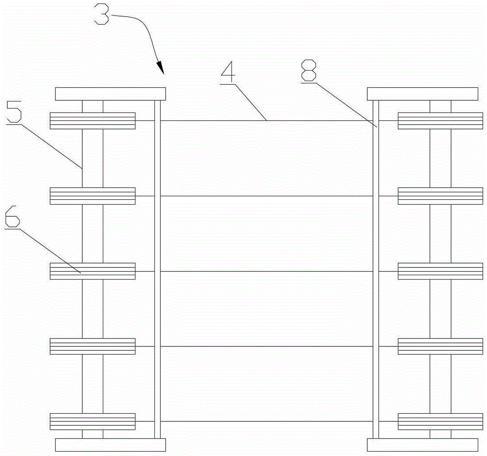
A plasma deposition and etching system
An etching system and plasma technology, used in semiconductor/solid-state device manufacturing, gaseous chemical plating, coating, etc., can solve problems such as poor compatibility, increase the bias power supply control system, and meet the needs of etching functions , the effect of improving heating efficiency and heating stability
- Summary
- Abstract
- Description
- Claims
- Application Information
AI Technical Summary
Problems solved by technology
Method used
Image

Examples
Embodiment 4
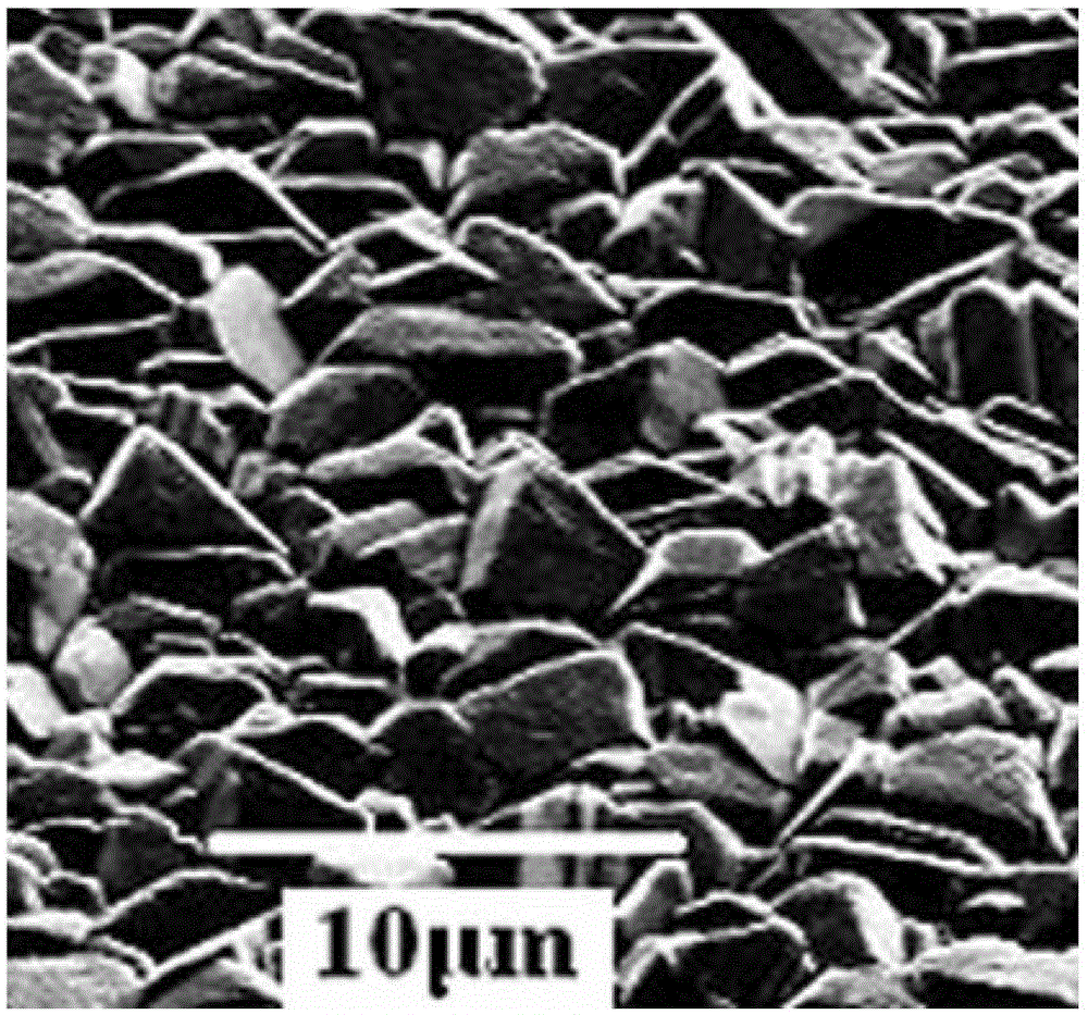
[0065] This embodiment provides a preparation process of a silicon surface nanocone structure. The equipment used is the plasma deposition and etching system mentioned in Embodiment 1. The difference is that the control methods of the system are different. The specific steps include: specific steps include:
[0066] (1) Take n-type silicon (100), and perform ultrasonic cleaning in acetone, ethanol and deionized water in sequence;
[0067] (2) After the silicon wafer is air-dried, put it into the reaction chamber for etching;
[0068] (3) Vacuum the cavity to close to 10 -2 Torr, then re-inflate to 20Torr, methane / hydrogen flow ratio is 0 / 100;
[0069] (4) Add filament current, adjust the filament voltage so that the temperature is about 2100°C, adjust the distance between the filament and the substrate so that the substrate temperature is about 800°C, turn on the power supply of the upper grid, and adjust the voltage so that the distance between the upper grid and the filame...
Embodiment 5
[0074] This embodiment provides a preparation process of a silicon surface nanocone structure. The equipment used is the plasma deposition and etching system mentioned in Embodiment 1. The difference is that the control methods of the system are different. The specific steps include:
[0075] (1) Take the newly prepared porous silicon and perform ultrasonic cleaning in acetone, ethanol and deionized water in sequence. In order to prevent the damage of the porous structure, the ultrasonic time of porous silicon is relatively short;
[0076] (2) After the silicon wafer is air-dried, put it into the reaction chamber for etching;
[0077] (3) Vacuum the cavity to close to 10 -2 Torr, then re-inflate to 20Torr, methane / hydrogen flow ratio is 0 / 100;
[0078] (4) Add filament current, adjust the filament voltage so that the temperature is about 2100°C, adjust the distance between the filament and the substrate so that the substrate temperature is about 800°C, turn on the power suppl...
PUM
| Property | Measurement | Unit |
|---|---|---|
| radius | aaaaa | aaaaa |
Abstract
Description
Claims
Application Information
 - R&D
- Intellectual Property
- Life Sciences
- Materials
- Tech Scout
- Unparalleled Data Quality
- Higher Quality Content
- 60% Fewer Hallucinations
Browse by: Latest US Patents, China's latest patents, Technical Efficacy Thesaurus, Application Domain, Technology Topic, Popular Technical Reports.
© 2025 PatSnap. All rights reserved.Legal|Privacy policy|Modern Slavery Act Transparency Statement|Sitemap|About US| Contact US: help@patsnap.com