
Three-dimensional Cu2S@ZnO nanometer heterostructure semiconductor material and preparation method thereof

A nano-heterostructure, semiconductor technology, applied in the direction of nanotechnology, nanotechnology, chemical instruments and methods, etc., can solve the problems of inapplicability to large-scale industrial production, high production costs, harsh reaction conditions, etc., and meet the requirements of reducing equipment , low cost and simple method

Inactive Publication Date: 2013-07-17
EAST CHINA NORMAL UNIV
View PDF1 Cites 18 Cited by
  • Summary
  • Abstract
  • Description
  • Claims
  • Application Information

AI Technical Summary

Problems solved by technology

However, most of the existing preparation methods have harsh reaction conditions and high production costs, which are not suitable for large-scale industrial production.

Method used

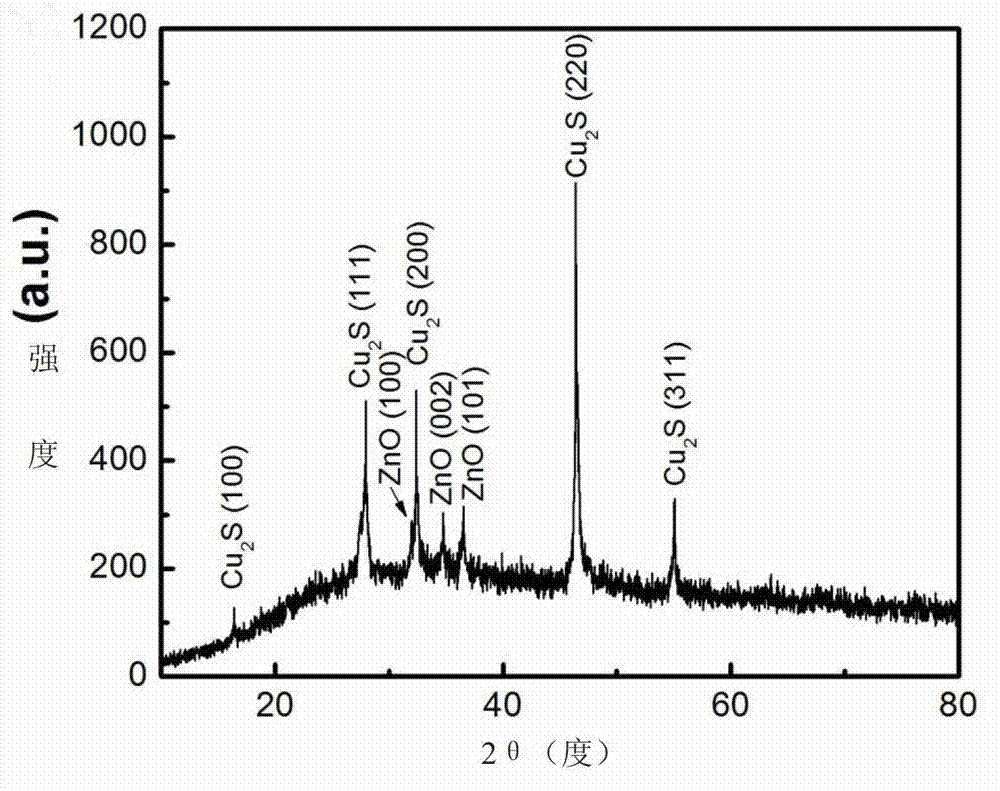
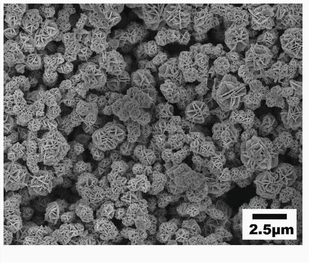
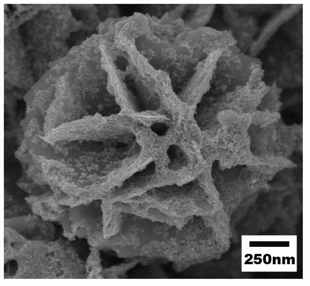

Image

  • Three-dimensional Cu2S@ZnO nanometer heterostructure semiconductor material and preparation method thereof
  • Three-dimensional Cu2S@ZnO nanometer heterostructure semiconductor material and preparation method thereof
  • Three-dimensional Cu2S@ZnO nanometer heterostructure semiconductor material and preparation method thereof

Examples


Embodiment

[0029] In this example, the three-dimensional Cu 2 The specific preparation steps of SZnO nano-heterostructure semiconductor material are as follows:

[0030] a. Mix 0.5g of cuprous chloride, 0.4g of thiourea and 0.25g of PVP, dissolve in 40mL of 95% ethanol and stir thoroughly for 30 minutes.

[0031] b. Then transfer the mixed solution into a 50mL reaction kettle, place the reaction kettle in a vacuum oven and heat it at 180°C for 6h, when the reaction is finished and cool to room temperature, collect the black reaction product and wash it repeatedly with absolute ethanol and deionized water several times.

[0032] c. Dry the pure sample in a vacuum oven at 60°C for use. Among them, the sample here refers to Cu 2 S sample, that is, the prepared flower-like Cu 2 S nanostructured substrate materials.

[0033] d. Add 10mL of urea solution (2M) dropwise to 10mL of ZnCl (0.5M), then dissolve it in 80mL of deionized water, stir the mixed solution magnetically for 30min and th...


PUM

PropertyMeasurementUnit
diameteraaaaaaaaaa
diameteraaaaaaaaaa
thicknessaaaaaaaaaa

Abstract

The invention discloses a three-dimensional Cu2S@ZnO nanometer heterostructure semiconductor material. The three-dimensional Cu2S@ZnO nanometer heterostructure semiconductor material comprises ZnO nanometer-particle crystals and a CU2S nanometer-flower structure substrate material, wherein the ZnO nanometer-particle crystals are uniformly covered on the CU2S nanometer-flower structure substrate material; the CU2S nanometer-flower structure substrate material consists of Cu2S nanometer-sheets; and a P-N junction is formed at the interface of the ZnO nanometer-particle crystals and the Cu2S nanometer-flower structure. The invention further discloses a preparation method of the three-dimensional Cu2S@ZnO nanometer heterostructure semiconductor material. The preparation method comprises the following steps of: synthesizing the Cu2S nanometer-flower crystals and ZnO nanometer-particle crystals by adopting a hydrothermal synthesis method, respectively; and uniformly compounding the ZnO nanometer particles on the Cu2S nanometer-sheets by using PEI (Polyether Imide) as an auxiliary material to obtain the three-dimensional Cu2S@ZnO nanometer heterostructure semiconductor material. The three-dimensional Cu2S@ZnO nanometer heterostructure semiconductor material has the advantages of being low in cost, low in growth temperature, high in repeatability and the like, and also has great development application potential in the on-spot emission field and the photo-catalysis field.

Description

technical field [0001] The invention relates to the technical field of optoelectronic materials, semiconductor materials and devices, in particular to a Cu 2 Cu fabricated from S nanoflower crystals and ZnO nanoparticle nanounits assisted by PEI 2 A semiconductor material of SZnO nano-heterostructure, and a preparation method for obtaining a large-area structure of this structure by a hydrothermal method without a catalyst. Background technique [0002] Cu 2 S is a P-type narrow bandgap semiconductor material with a direct bandgap of 1.2eV and good conductivity. Due to its unique electrical, chemical and optical properties, Cu 2 S has extensive research and application in solar cells, photocatalysis, field emission, sensors and other fields. Zinc oxide (ZnO), as an N-type wide bandgap (Eg=3.37eV), is a cheap, low-toxic semiconductor material, and has been widely used in combination with other narrow bandgap semiconductor materials to study its new properties . Recently...

Claims


Application Information

Patent Timeline
Patent Type & Authority Applications(China)
IPC IPC(8): C01G3/12C01G9/02B01J27/04B82Y40/00B82Y30/00
Inventor 李守川郁可汪阳宋长青尹海宏朱自强
Owner EAST CHINA NORMAL UNIV
Learn More