Block RAM (random-access memory) with multiple Write-Modes in FPGA (field programmable gate array)

A technology for writing patterns and input bits, which is applied in information storage, static memory, digital memory information, etc., can solve problems affecting chip operating frequency, large skew time, reliability errors, etc., to achieve both high speed and reliability, The effect of guaranteeing functional correctness

Active Publication Date: 2013-07-10
FUDAN UNIV
View PDF3 Cites 6 Cited by
  • Summary
  • Abstract
  • Description
  • Claims
  • Application Information

AI Technical Summary

Problems solved by technology

This requires less logic circuit design, but because the control signal transmission distance is longer, the skew time is longer, and Write_Mode has high requirements on the timing of the signal, so it may cause timing reliability errors
In addition, when the circuit works in different working environments (process angle, temperature, voltage, etc.), the delay of the signal is difficult to simulate with a fixed delay unit, because it is necessary to take the delay to ensure that the data can be written correctly in all cases The maximum value of , making the application of BRAM in the actual chip greatly affects the operating frequency of the chip

Method used


Image

  • Block RAM (random-access memory) with multiple Write-Modes in FPGA (field programmable gate array)
  • Block RAM (random-access memory) with multiple Write-Modes in FPGA (field programmable gate array)
  • Block RAM (random-access memory) with multiple Write-Modes in FPGA (field programmable gate array)

Examples


Embodiment Construction

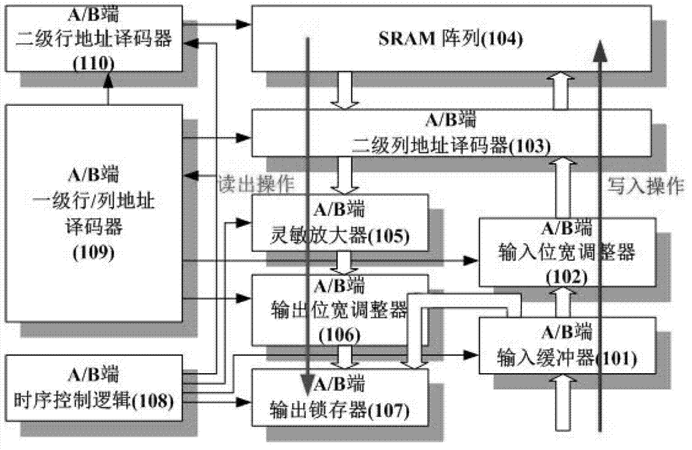
[0022] For output data, the most important timing is in the second column decoding module 103 and sensitive amplifier modules 105 superior. Because the secondary column decoding module 103 is a bidirectional channel for selective input / output of control data, while the sensitive amplifier module 105 It is to differentially amplify the analog waveform signal read from the SRAM to generate a standard digital signal and latch it, so as to ensure the correct transmission of data.

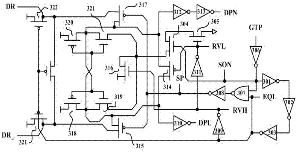
[0023] Sensitive Amplifier Module 105 Such as image 3 shown. The combined circuit part on the right is used to generate various control signals, mainly controlling the delay between signal circuits. Of particular note are the three rightmost inverters ( 301 , 302 , 303 ), which is used to generate a delay so that the SON signal turns on the corresponding MOS tube earlier than the RVL signal. The situation in which this is done is that the two sets of NMOS transistors ( 305 , 306 ) only in t...


PUM


Abstract

The invention belongs to the technical field of electronics, and in particular relates to a sequential control circuit design of write-in operation of IP (Internet protocol) hard core Block RAM (random-access memory) embedded in an FPGA (field programmable gate array). The standard shows sequential control situation requirements under corresponding Write-Modes, and meanwhile, discloses that a delay situation in a current working environment is obtained through a dynamic redundant circuit simulation technique and is fed back to a Write_Mode control module, thereby implementing a configurable circuit design of write operation in different working environments with the different Write-Modes. According to the invention, the required three different Write-Mode configuration conditions in the Block RAM design can be realized, and the high-speed property and reliability of a circuit under various working states are ensured fully.

Description

technical field [0001] The invention belongs to the technical field of electronic design, and in particular relates to the realization of write operation sequence control in FPGA embedded IP hard core Block RAM (hereinafter referred to as BRAM) and the circuit design taking into account high speed and reliability. Background technique [0002] Early FPGAs consisted of configurable logic blocks (CLBs), input / output blocks (IOBs) and interconnect resources. However, modern digital circuit design has higher and higher requirements for storage resources in FPGA, and using CLB configuration to implement storage functions will consume a large number of configurable resources, and the realized performance will be affected by resource distribution and interconnection length. Therefore, the BRAM IP hard core is introduced into the FPGA to support the realization of storage resources in the FPGA, to solve the performance and function limitations of the logic resources, and to make the...

Claims


Application Information

Patent Timeline
Patent Type & Authority Applications(China)
IPC IPC(8): G11C7/10
Inventor 张昕睿王健陈丹来金梅
Owner FUDAN UNIV
Why Eureka
Try Eureka