Micro machining method for bulk silicon for forming cavity structure of MEMS (micro-electromechanical systems) thermopile detector

A technology of thermopile detectors and processing methods, which is applied in the direction of microstructure technology, microstructure devices, and manufacturing microstructure devices, etc., which can solve the problems of low smoothness of inner surface, reduction of symmetry of thermopile structure, and uncontrollable lateral undercutting and other issues to achieve the effect of strong manufacturability and high controllability

Active Publication Date: 2013-06-12
中科芯未来微电子科技成都有限公司
View PDF6 Cites 7 Cited by
  • Summary
  • Abstract
  • Description
  • Claims
  • Application Information

AI Technical Summary

Problems solved by technology

The disadvantage of this method is that the lateral undercutting is uncontrollable, the smoothness of the inner surface is low, and the symmetry of the thermopile structure is reduced

Method used


Image

  • Micro machining method for bulk silicon for forming cavity structure of MEMS (micro-electromechanical systems) thermopile detector
  • Micro machining method for bulk silicon for forming cavity structure of MEMS (micro-electromechanical systems) thermopile detector
  • Micro machining method for bulk silicon for forming cavity structure of MEMS (micro-electromechanical systems) thermopile detector

Examples


Embodiment Construction

[0018] The present invention will be further described below in conjunction with specific drawings and embodiments.

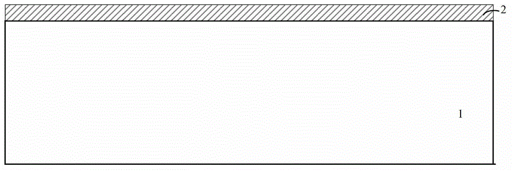
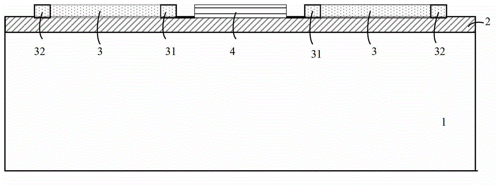
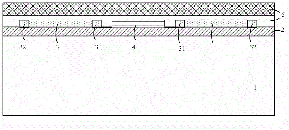
[0019] The structure of the infrared thermopile detector with cavity structure proposed by the present invention is as follows: Figure 6 As shown, a silicon dioxide (SiO2) film 2 is thermally oxidized and grown on a silicon substrate 1, and a thermopile region 3 and an infrared absorption region 4 are formed on the silicon dioxide film 2. The thermopile structure can take various forms such as a circular , rectangle, etc. One end of the thermopile region 3 close to the infrared absorption region 4 is a hot junction region 31 , and the other end away from the infrared absorption region 4 is a cold junction region 32 . A composite film structure 5 of silicon nitride and silicon dioxide is deposited on the thermopile structure layer, and an opening 6 is photolithographically etched on the composite film. The release channel 61 of the thermopile structure is for...


PUM


Abstract

The invention provides a micro machining method for bulk silicon for forming a cavity structure of an MEMS (micro-electromechanical systems) thermopile detector. The method comprises the following steps of: providing a silicon substrate, growing a silica membrane on the silicon substrate in a thermal oxidation manner, and forming a thermopile area and an infrared absorption area on the silica membrane. A thermal nodal area is arranged at one end of the thermopile area, close to the infrared absorption area, and a cold nodal area is arranged at the other end of the thermopile area, far away from the infrared absorption area. A silicon nitride and silica compound membrane structure is deposited on a thermopile structure layer, and a corrosion opening is formed in a compound membrane through photoetching. A release channel of the thermopile structure is formed by the corrosion opening. Through the release channel, a superficial layer on the surface of the bulk silicon is corroded by using an isotropy corrosion method so as to form a thin cavity of the superficial layer of the bulk silicon, and a bulk silicon deep layer below the thin cavity is corroded by using an anisotropy corrosion method so as to form a regular smooth ladder-shaped cavity structure, and therefore, the cavity structure in the bulk silicon is finally formed. The cavity structure formed by using the method has a regular and smooth inner surface and is good in structure symmetry.

Description

technical field [0001] The invention relates to a bulk silicon micromachining technology for forming a MEMS cavity structure, which is especially suitable for the manufacture of thermopile infrared detectors. Background technique [0002] Infrared detectors are one of the most critical components in an infrared system. The thermopile infrared detector is an uncooled infrared detector developed earlier. Its working principle is based on the Seebeck effect, in which a temperature difference between two different electrical conductors or semiconductor materials results in a voltage difference between the two materials. Because thermopile infrared detectors have the advantages of small size, can work at room temperature, wide-spectrum infrared radiation response, can detect constant radiation, and low manufacturing cost, they are widely used in safety monitoring, medical treatment, life detection, etc. [0003] At present, the thermopile structure generally adopts a thin film ...

Claims


Application Information

Patent Timeline
Patent Type & Authority Applications(China)
IPC IPC(8): B81C1/00
Inventor 孟如男王玮冰
Owner 中科芯未来微电子科技成都有限公司
Why Eureka
Try Eureka