Electric conduction plug and forming method

A conductive plug and semiconductor technology, applied in circuits, electrical components, electrical solid devices, etc., can solve problems such as inability to control MOS transistors, and achieve the effects of improving device performance, easily controlling etching time, and reducing process steps.

Active Publication Date: 2013-05-22
SEMICON MFG INT (SHANGHAI) CORP
View PDF6 Cites 3 Cited by
  • Summary
  • Abstract
  • Description
  • Claims
  • Application Information

AI Technical Summary

Problems solved by technology

[0005] However, since the nanowire active region of the multi-gate field effect transistor is parallel to the plane of the semiconductor substrate, the electrical interconnection between the nanowire active region and the metal interconnection layer of the prior art requires an active region perpendicular to the nanowire. Conductive plugs in the source area, but the direct formation of conductive plugs will electrically connect the active areas of nanowires of different heights, and cannot independently control the MOS transistor corresponding to the active area of ​​each nanowire

Method used


Image

  • Electric conduction plug and forming method
  • Electric conduction plug and forming method
  • Electric conduction plug and forming method

Examples


Embodiment Construction

[0053] The method for forming the multi-gate field effect transistor in the prior art specifically includes:

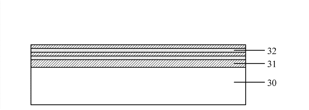
[0054] Please refer to figure 2 , providing a semiconductor substrate 30, on which silicon germanium layers 31 and silicon layers 32 are alternately formed, and impurity ions are doped in the silicon layers 32;

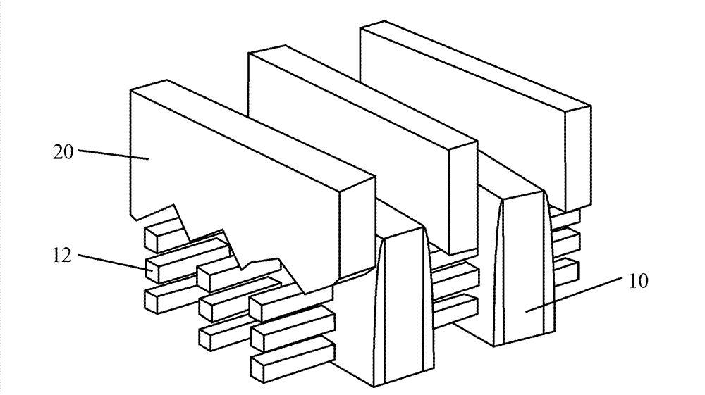
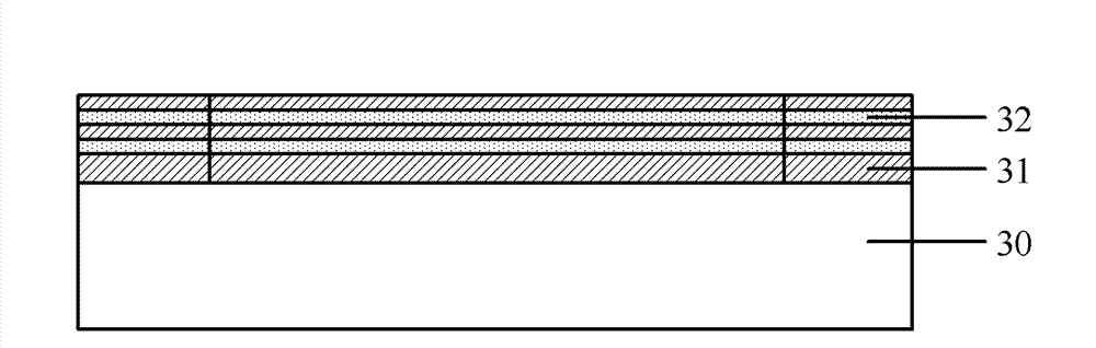
[0055] Please refer to image 3 and 4 , the Figure 4 for image 3 A schematic diagram of the three-dimensional structure, etching the silicon germanium layer 31 and the silicon layer 32 in some areas to form a fin-shaped stacked structure of the silicon germanium layer 31 and the silicon layer 32;

[0056] Please refer to Figure 5 , the silicon germanium layer 31 is wet-etched to remove the silicon germanium layer 31 in the laminated structure of the fin-shaped silicon germanium layer 31 and the silicon layer 32, and the silicon layer between the silicon germanium layers 31 forms a nanometer A wire active region 33, forming a gate dielectric layer (n...


PUM


Abstract

An electric conduction plugs comprises a semiconductor substrate, a gate structure which is positioned on the surface of the semiconductor substrate, a plurality of nanowire active areas and a dielectric layer, grooves, dielectric materials, and electric conduction plugs, wherein the plurality of nanowire active areas are penetrated through the gate structure and are parallel to the semiconductor substrate, the dielectric layer is positioned on the surface of the semiconductor substrate and covers the gate structure and the nanowire active areas, the interval spaces among the nanowire active areas are fully filled by the dielectric layer, the grooves are positioned on two sides of the gate structure, inclined angles are arranged on the side walls of the grooves, the grooves are enables the nanowire active areas to be provided with etched sections, the dielectric materials are used for filling the grooves, the electric conduction plugs are arranged in the dielectric materials, and each electric conduction plug is connected with the corresponding nanowire active area. Due to the fact that the etched sections, with the different heights, of the nanowire active areas are arrayed in a ladder mode, the electric conduction plugs are connected between two ends of each nanowire active area and a metal mutual-connection layer, voltages and currents at two ends of each nanowire active area can be controlled, and improvement of device performance is benefited.

Description

technical field [0001] The invention relates to semiconductor manufacturing technology, in particular to a conductive plug connected with a nanowire active area and a forming method. Background technique [0002] With the continuous development of semiconductor process technology, a gate-last (gate-last) process has been widely used to obtain an ideal threshold voltage and improve device performance. However, when the feature size (CD, Critical Dimension) of the device is further reduced, even if the gate-last process is adopted, the structure of the conventional MOS field effect transistor can no longer meet the requirements for device performance, and the multi-gate device is obtained as a substitute for the conventional device. received widespread attention. [0003] Multi-Gate Field Effect Transistor (MuGFET) is a common multi-gate device, figure 1 A schematic diagram of a three-dimensional structure of a multi-gate field effect transistor in the prior art is shown. S...

Claims


Application Information

Patent Timeline
Patent Type & Authority Applications(China)
IPC IPC(8): H01L23/522H01L21/768
Inventor 何其旸
Owner SEMICON MFG INT (SHANGHAI) CORP
Why Eureka
Try Eureka