
Light-emitting diode (LED) packaging structure

A technology of LED packaging and LED chips, which is applied in the direction of electrical components, circuits, semiconductor devices, etc., can solve the problems of high thermal resistance TG point, unfavorable stability of device heat dissipation and physical characteristics, complex structure, etc., to achieve efficient heat dissipation and efficient heat dissipation The effect of cost control

Inactive Publication Date: 2013-05-15
孙雪刚
View PDF6 Cites 6 Cited by
  • Summary
  • Abstract
  • Description
  • Claims
  • Application Information

AI Technical Summary

Problems solved by technology

Secondly, the internal basic structure of silver glue after curing is epoxy resin skeleton + silver powder filled thermal and conductive structure. The stability of heat dissipation and physical properties is extremely unfavorable, and the structure is complex

Method used


Image

  • Light-emitting diode (LED) packaging structure

Examples


Embodiment

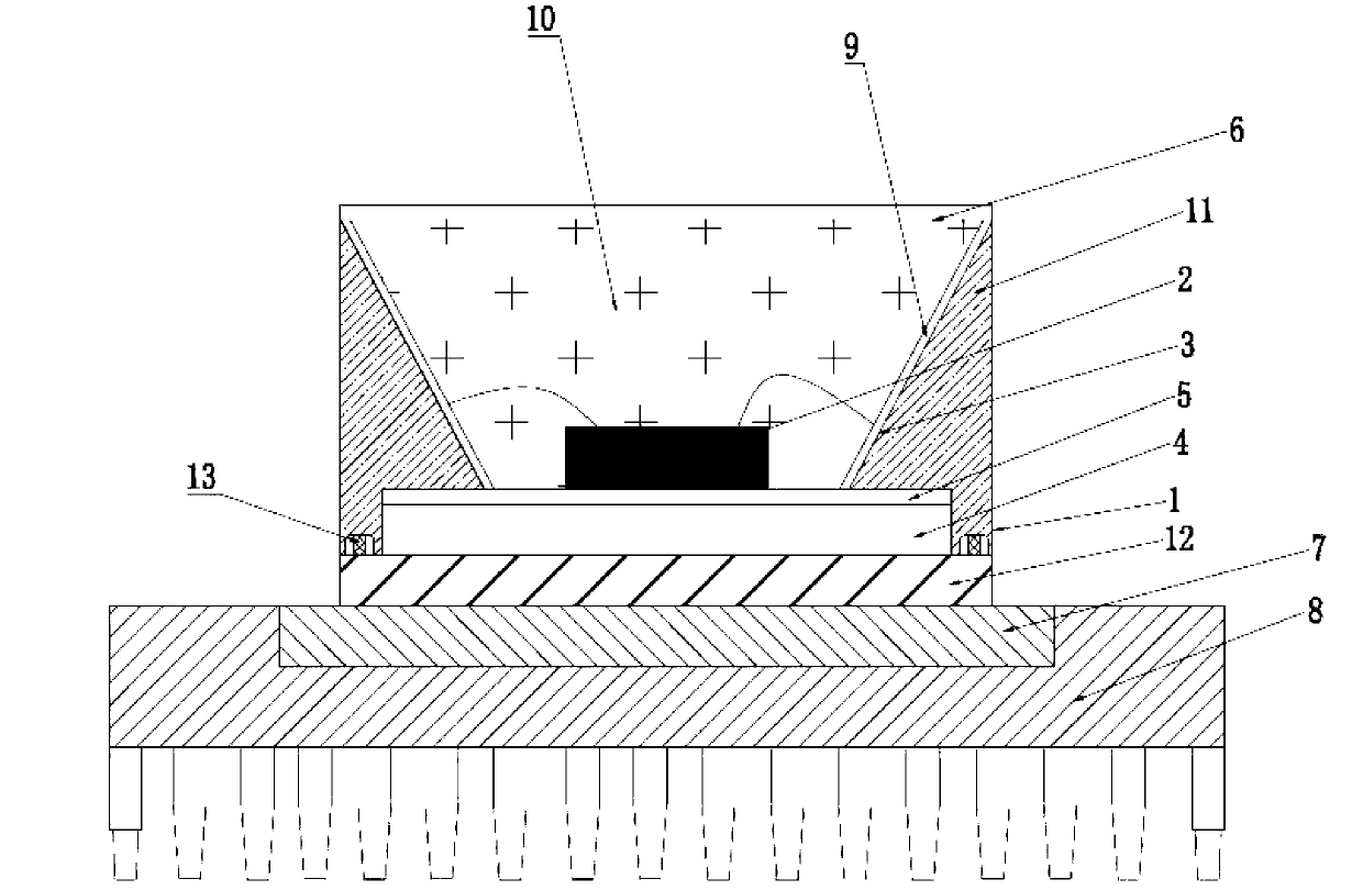
[0021] Such as figure 1 As shown, an LED packaging structure includes a packaging substrate 1 and a light-emitting LED chip 2. The packaging substrate 1 has at least one groove-shaped reflective cup 3, the LED chip 2 is mounted on the packaging substrate 1, and the light-emitting LED A thermally conductive substrate 4 is arranged between the chip 2 and the packaging substrate 1, the thermally conductive substrate 3 uses a silver base as a thermal lining material, and the thermally conductive substrate is welded to the packaging substrate through a tin sheet 5.

[0022] The upper end of the reflecting cup is provided with a lens 6, the lens 5 and the reflecting cup 3 form a sealed cavity, and the lens is a glass sheet containing phosphor. By arranging a focusing lens on the surface of the LED chip and placing the phosphor-containing glass sheet at a certain distance from the wafer, not only the reliability of the device is improved, but also the light efficiency is greatly improve...


PUM


Abstract

The invention discloses a light-emitting diode (LED) packaging structure which comprises a packaging base plate and an LED chip. The packaging base plate is provided with at least one reflecting cup which is groove-shaped. A heat conducting substrate is arranged between the LED chip and the packaging base plate. A silver base is adopted by the heat conducting substrate to serve as a heat lining material. The heat conducting substrate is fixedly connected with the packaging base plate through tin soldering. Heat emitted by an LED is rapidly conducted through heat absorption copper blocks. Due to the fact that the copper blocks are added between a radiator which is made of aluminum, and the LED, a heat dissipation effect is further strengthened. Due to the fact that tin pieces serve as connecting materials between crystal particles and a heat lining, a heat conducting effect is further strengthened. In addition, cost performance of the radiator is fully taken into consideration, radiators with different characteristics are combined together, and efficient heat dissipation is achieved, the LED packaging structure is reasonable in cost control and simple in structure, and the LED packaging structure improves a lighting effect.

Description

Technical field [0001] The present invention relates to a semiconductor light emitting device, in particular to a packaging structure that effectively dissipates the heat generated during the operation of the semiconductor light emitting element LED. Background technique [0002] In recent years, with the development of high-power white light LED packaging technology, LED packaging has successively experienced development stages such as bracket type (Lamp LED), patch type (SMD LED), and power LED (Power LED). With the increase of chip power, especially the demand for the development of solid-state lighting technology, new and higher requirements are put forward on the optical, thermal, electrical and mechanical structures of LED packages. Among them, heat dissipation is very important for power LED devices. If the heat generated by the current cannot be dissipated in time and the junction temperature of the PN junction is kept within the allowable range, it will not be possible ...

Claims


Application Information

Patent Timeline
Patent Type & Authority Applications(China)
IPC IPC(8): H01L33/64H01L33/48
Inventor 孙雪刚
Owner 孙雪刚
Learn More